
Performance Validation of 300MB/s: ARM-FPGA Interconnect via DSMC Bus on RK3572 Platform
In industrial automation and high-speed data acquisition, ARM-FPGA co-design is common, but their communication interfaces face a trade-off: SPI is too slow (~10 Mbps), while PCIe is overkill with high complexity and cost.
Forlinx Embedded addresses this with a cost-effective solution using Rockchip’s DSMC (Double Data Rate Serial Memory Controller) bus. Test results show stable read/write bandwidth exceeding 300 MB/s, offering a new approach to industrial communication bottlenecks.
1. Test Platform: ARM+FPGA Integrated Evaluation Board
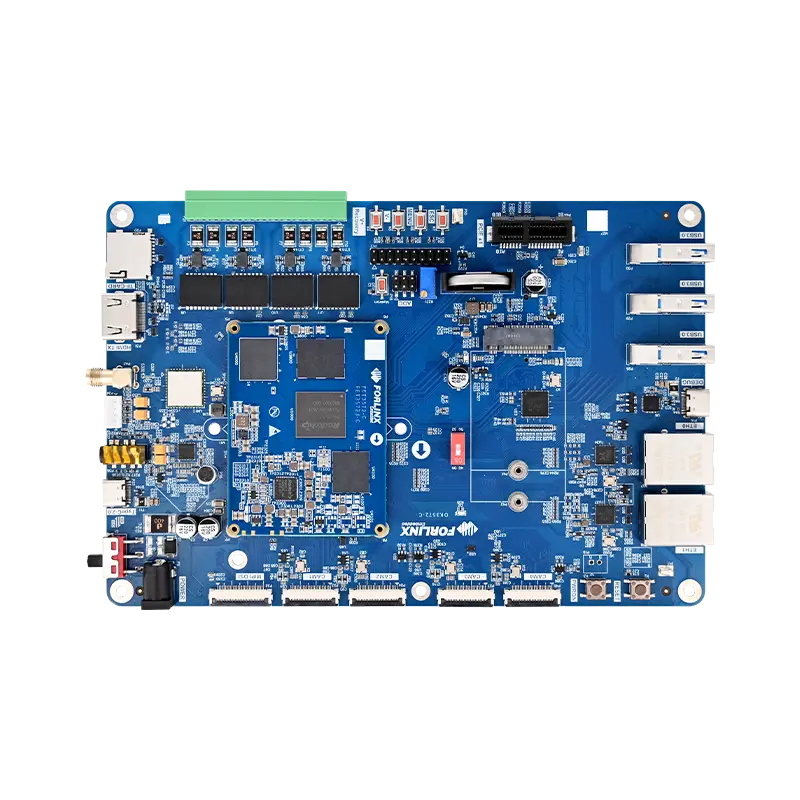
Forlinx Embedded has independently developed an FPGA+ARM integrated test board to precisely assess the performance of ARM-FPGA communication interfaces while eliminating signal degradation and throughput loss typically caused by traditional wiring methods.
It supports four SoMs (RK3572, RK3576, RK3568, RK3506) and seamlessly integrates FPGA cores from vendors like Xilinx, Anlogic, and Gowin, offering a stable, reliable hardware base for heterogeneous computing performance validation.
Supported interconnect interfaces per platform are as follows:
| Interface Type | RK3572 | RK3576 | RK3568 | RK3506 |
| SPI | Support | Support | Support | Support |
| PCIE 2.1X1 | Support | Support | Support | Not Supported |
| DSMC | Support | Support | Not Supported | Support |
| SDIO | Support | Support | Support | Support |
| MAC | Support | Support | Support | Support |
| FSPI | Not Supported | Not Supported | Support | Support |
| LCDC | Support | Support | Not Supported | Support |
| FLEXBUS | Not Supported | Support | Not Supported | Support |
2. DSMC Communication Architecture and Testing Solution
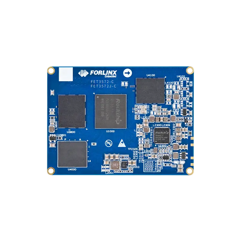
This test utilizes the Forlinx Embedded development board to verify the communication performance between the FET3572-C SoM and the FPGA via the DSMC bus.
2.1 Basic Test Environment
Development Environment: Windows 10/11 64-bit; VMware 15 with Ubuntu 22.04 (Please refer to the Forlinx official website RK3572 development environment setup guide).
System Version: U-Boot-2025.04, Linux Kernel 6.12.58, Buildroot 2025.02.7
Hardware Platform: FET3572x-C_FPGA_Test V1.0 Industrial Development Board
Architecture Mode: RK3572 acts as the DSMC host, and the FPGA acts as the DSMC slave.
2.2 Bandwidth Test Results
| Item | Theoretical Speed | Actual Test Result |
| DSMC-FPGA Test | Read Speed: 400MB/S | Read Speed: 304MB/S |
| Write Speed: 400MB/S | Write Speed: 303MB/S |
2.3 ARM-Side Implementation Logic
On the ARM side, a Linux application initiates read/write requests via the /dev/dsmc/cs0 device node. The DSMC driver in the kernel receives the command and invokes the CPU_DMA engine. The DMA_MMP module then facilitates direct data movement between DDR memory and the DSMC_IO hardware interface, eliminating CPU involvement in data copying and ensuring high throughput and low latency.
The testing program can perform read/write verification by configuring parameters such as packet size and loop count, and outputs the bit error rate and measured transmission rate.
2.4 FPGA-Side Implementation Logic
The FPGA side implements the Local Bus Slave function:
- Data Reception from ARM: Data is sampled via IOBUF and IDDR before being stored in DRAM.
- Data Transmission to ARM: Data from DRAM is output to the DSMC bus via ODDR and IOBUF for data return.
2.5 System Architecture Diagram
The overall architecture consists of two layers: the ARM side and the FPGA side.
ARM Side: The path from user-space application to the underlying hardware interface sequentially includes the Linux application, device node, driver layer, DMA engine, and DSMC hardware I/O.
FPGA Side: Correspondingly implements data sampling, storage, and return logic.
High-speed interaction is achieved between the two ends via the DSMC bus.
3. Test Demonstration: Stable Transfer, Zero Bit Error
This test is conducted using the dsmc_mmap_test tool, which allows flexible configuration of parameters such as transmission mode, loop count, payload length, and clock frequency. The core parameters are described as follows:
Execute:./dsmc_mmap_test -c 1000 -l 65528 -v -p
-o, --op. operation: rw (write+read+verify, default), wo (write only), ro (read only)
-c, --cycle.transfer count
-l, --length. payload bytes per transfer (12-byte preamble added automatically
-G, --gen_mode. data pattern 0=random 1=sequential
-v, --verbose. dump write/read data
-P, --perf. print performance (MiB/s) summary
-f, --freq. set DSMC IO clock freq in Hz (e.g. 100000000)
This test selected a payload size of 65,528 bytes (to avoid potential overflow issues at 65,536 bytes) and performed 100-cycle and 1000-cycle read/write verification tests, with results as follows:
100-Cycle Read/Write Test
Test Command: ./dsmc_mmap_test -c 100 -l 65528 -v -P
Transfer Mode: Read/Write with Verification
Test Result: 100 cycles completed successfully; 0 failures, 0 bit errors; Bit Error Rate: 0.0000%
Performance: Average Write Speed: 303.10 MiB/s, Average Read Speed: 305.59 MiB/s
1000-Cycle Read/Write Test
Test Command: ./dsmc_mmap_test -c 1000 -l 65528 -v -P
Transfer Mode: Read/Write with Verification
Test Result: 1000 cycles completed successfully; 0 failures, 0 bit errors; Bit Error Rate: 0.0000%
Performance: Average Write Speed: 303.53 MiB/s, Average Read Speed: 304.91 MiB/s
Both test sets demonstrate that the DSMC bus delivers stable performance in long-duration, high-volume data transfer scenarios. Read/write speeds consistently remain at the 300 MB/s level throughout testing, with a sustained bit error rate of 0. This fully meets the demands of industrial applications for high-speed, reliable communication.
The DSMC bus achieves near-PCIe level transmission performance with moderate development cost and hardware requirements, making it perfectly suited for medium-to-high-speed industrial interconnection scenarios. The Forlinx Embedded FET3572-C SoMs have completed comprehensive DSMC interface adaptation and validation, enabling customers to accelerate the development of heterogeneous computing products such as industrial PLCs, multi-axis motion control systems, and high-speed data acquisition solutions.