Development Demonstration of PRU of AM5718
Overview:
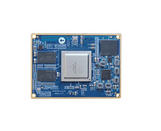
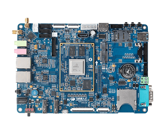
Forlinx OK5718-C development board is designed based on TI AM5718 processor which contains two PRU-ICSS(ProgrammableReal-Time Unit Subsystem and Industrial Communication Subsystem), here we will have a demonstration of the PRU structure and how to do development and debug work by PRU.
PRUSS is a module that connects to L3_MAIN, similar with other modules like ARM and DSP, it can visit other peripherals.
PRUSS contains two PRUs, it connects to subsystem interrupt controller, instruction memory, data memory, shared memory and peripherals by its 32-bitinterconnect bus.
PRU is not an accelerator, it's a 32-bitLoad/Store RISC little-end processor, each PRU consists pf 32 registers (R0- R31), 12Kbyte instruction RAM, 8K byte data RAM and 32K byte shared RAM. Insruction RAM is separated and not accessable, but data RAM is accessiable by mapping address. Special 21 input pins and 21 output pins.
PRU-ICSS1 and PRU-ICSS2 have below features:
- • PD_L4PER power domain instantiation
- • two master ports (PRU0and PRU1 core initiators) on the device L3_MAIN interconnect
- • Non-wakeup capable - smart Standby protocol with the device PRCM
- • Software assertion of a standby request "MStandby" (formaster port clock disable) with local (PRUICSS) monitoring of thePRCM "MWait" acknowledge.
- • one slave(configuration) port on the L3_MAIN interconnect for device hosts(MPU, DSP1, etc.) to access various memories and registers ofPRU-ICSS
- • Non-wakeup capable - smart Idle protocol with thedevice PRCM
- • 10 output interrupt events from local interruptcontroller - PRUSS_INTC:
– 2events to each PRU core (events 0 and 1)
– 8 events mapped tothe device IRQ_CROSSBAR which further remaps them to deviceinterrupt
controllers (events 2 through 9)
– 2 eventsmapped to the device DMA_CROSSBAR, that remaps them to device DMAcontrollers
(events 8 and 9)
• 32 external interrupts aremapped via the device IRQ_CROSSBAR to the local PRUSS_INTC
• Alocal software gating of clocks to several modules within PRUsubsystem (local clock management
protocol), as follows:
–PRUSS_IEP
– PRUSS_eCAP_0
– PRUSS_UART0
–PRUSS_INTC
– PRUSS_PRU0
– PRUSS_PRU1
• 3 inputclocks obtained from device PRCM:
– a PRU-ICSS top levelgatable interface clock
– a PRUSS IEP functional clock
–a PRUSS UART0
• No memory/register retention is supported
• One hardware non-retention (level sensitive) reset
PART 1 PRU RAM Mapping
1.1 Instruction space
Separated space of each PRU is 0x00000000~0x00002FFF. The instruction space will be initialized by ARM/ DSP, program pointer on PC is a 32-bit word address, but not byte
address, for example, PC=2, it indicates the instruction address is 0x 08
1.2 Data space
Data RAM space of separted 8Kbyte of each PRU is 0x 0000~ 0x 01FF. Data RAM is mounted to internal bus of PRU subsystem, so it's accessable to other modules in the subsystem,
the mapping address of this space on the other PRU is 0x 2000- 0x 21FF. Shared interrupt controller register, PRU controller/ status register are also in the data space and have separated address spaces.
1.3 Global address space mapping
Base address(L3_MAINbase address) of PRU_ICSS1 local address in global address is 0x4B2A0000, and base address(L3_MAINbase address) of PRU_ICSS2 local address in global address is 0x4B28E000.
PRU can visit data space of PRUSS by local address or global address. Take global address by L3_MAINdevice to visit data space is slower than taking local address to visit data space.
External module of PRUSS, such as ARM and DSP can access to PRU sources by system global address space mapping port together with global address (OffsetAddress + L3_MAIN base
address). Details please refer to 30.4.4.2PRU-ICSS Global Memory Map of AM571xTechnical Reference Manual
PART 02 Control/ status register
Control/ status register of PRU0 is from 0x00020000 to 0x0002_3FFF, control/ status register address of PRU1 is from 0x0002_4000 to 0x0002_5FFF
2.1 PRU_CONTROL register
ARM/ DSP can control PRU status by control register
2.2 PRU_STATUS register
status register is the program pointer regiter of PRU, it would be some latency before program running.
2.3 PRU_WAKEUP_EN
Before executing SLP instruction to get into sleeping mode, enable WAKEUP bit, input 1 for R31 of the register, that means WAKEUP&R31!=0, PRU will be waken up.
2.4 PRU_CYCLE
when CONTROL[ENABLE]=1 and CONTROL[COUNTENABLE]=1,CYCLECNT will count time by PRU clock cycle. When CONTROL[ENABLE]=0 or CONTROL[COUNTENABLE]=0, timing stops. Re-enable it to recover counting.
2.5 STALLCNT
When CONTROL[ENABLE]=1 and CONTROL[COUNTENABLE]=1, also PRU is not able to take instructions, STALLCNT will start timing by PRU cycle, its value always less or equals the
CYCLECNT value.
2.6 PRUSS_DBG_GPREG 0~31
PRUSS_DBG_GPREG0~31 are matched with R0~R31, when PRU stops, ARM/ DSP read/ writer INTGPR0~31 will directly read/ writer R0~R31.
PART03 General register
3.1 PRU event/ R31
R31 is a special register with reading and writing functions. Write to R31, for example, write a channel number 0 to 15 to R31_PRU_VEC[3:0], meanwhile R31_PRU_VEC_VALID, it will generate related interrupt output event to interrupt controller event. Two PRU output same interrupt event or output to the same interrupt controller.
Read R31, R31[29:0] indicates the status of PRU_R30[29:0]. R31[31:30] indicates status of INTR_IN[0] and INTR_IN[1]
3.2 R30
Each PUR has 32 output pins PRU0_R31[31:0] and PRU1_R31[31:0], the value wrote to R30[31:0] will be directly output to PRUn_R31[31:0]
PART 04 PRU interrupt controller
The PRU interrupt controller can support 64 system events, 10 interrupt channels and 10 host machine interruptions
PRU-ICSS1_INTC/PRUSS2_INTC interrupt 0~31 are matched with events generated by PRU-ICSS. System events 16~31 is generated by writing to R31
PRU_ICSS system events 32~55 can choose standard or MII_RT event by configuring PRUSS_MII_RT[0], PRUSSEVTSEL=0 to choose PRU-ICSS special IRQ_CROSSBAR output event as interrupt source, set PRUSSEVTSEL=1 to choose event generated by MII_RT as interrupt source.
10 channels could be mapped by any 64 system events, multiple system events could map to one channel, but please don't map one system event to multiple channels.
Set PRUSS_INTC_CMR to get maps of channels and 64 system events, PRUSS_INTC_CMRi(i is 0~15) is used for making i*4 to i*4+k system events map to same channel. Take channel
number set y related register bit to map to related system event.
10 host machine interrupt and 10 channels could be mapped each other, multiple system events could map to one channel, but please don't map one system event to multiple
channels.
PRUSS_INTC_HMRi(i is 0~3)is used for mapping channel 0-9 to host machine interrupt 0- 9. Configure register bit to set host machine interrupt, build mapping between interrupt and channel.
Host machine interrupt 0 outputs to R31.b30, interrupt 1 outputs to R31.b31, interrupt 2~ 9 output PRUSS to PRUSS_EVTOUT0~7 of ARM and DSP. Interrupt vector table is not
supported by PRU, generated 0, 1 could be used for PRU waking up or status checking.
PART 05 PRU code pack
Forlinx kindly provides PRU demo source code to users
PART 06 Software debug
6.1 debug tool
USBJTAG emulater XDS100V2 ,XDS100V2 are kindly recommended.
6.2 Hardware connection
1. Connect XDS100V2 emulater with Forlinx OK571-C development board as below
2. Connect XDS100V2 with USB of PC via USB cable
6.3 Debug
Here we will use Forlinx PRU demo to do PRU_LED0 debug, import the project to CCS, right click PRU_LED0 to choose Properties
Choose related emulater and compilier version, after all settings, please click OK
Right click PRU_LED0,choose DebugConfigurations
Choose PRU_LED0, delete realted check box as below, click Apply and then Debug
Run-> debug
get into debug as below
Below indicates compiling is successful
Cursor will stop at the main function after getting into debug mode
During debug, users can take below operation to check variable and register value Click view menu, choose Expressions option
get below interface
Choose target variable name, right click AddWatch Expression
Then OK
Add GPIO value to Expressions
Click Addnew expression to input R30, and it will be whown on Expressions
Get into debug interface, when program run to a certain line, right click this line, and click runto line, then it will run to this line, right click line 57
Run to line 57 and GPIO value will change to hexadecimal as 0xffffffff
Right click line 60, choose runto line, R30 value will change