What is pin multiplexing?
What is pin multiplexing?
Pin reuse, also known as pin multiplexation, pin reuse, pin reuse, pin remapping, and so on.
Why pin reuse?
Normal systems, especially embedded systems, when the chip is designed, there is enough space, enough pin resources to use, different pins, will not coincide, are separate, each has its own role. For example, a certain pin, is the corresponding USB of those pins, a certain pin is the corresponding SD card of those pins and so on.
Pin reuse may occur when the pin resources on the chip are not sufficient, and on the chip, pin reuse may occur in order to make more efficient use of the pin resources. Physically, the same set of pins, pins, can be set (through the software configuration of the corresponding registers to control) for different functions so that it can be implemented according to actual needs, in different cases, the use of the same set of pins, to achieve different functions for different functions.
Pin multiplexing issues are described
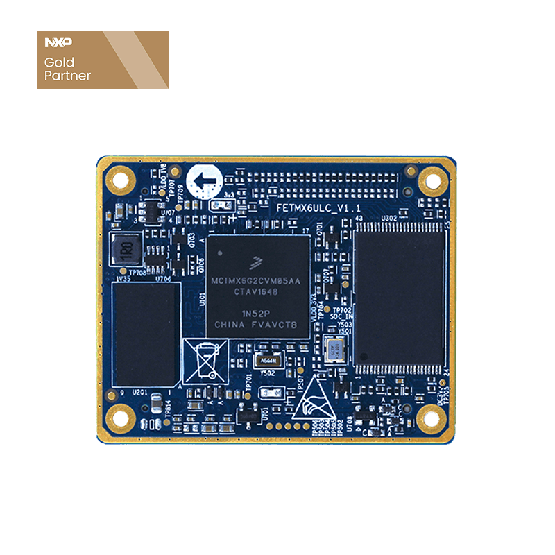
CPU functions are becoming more and more abundant, and Forlinx brochures are all a parameter table for the core board, one parameter base board. The core board parameter table supports more parameters than the base plate, which is pin multiplexing. Take, for example:
Serial 1, SD card, CAN, IIC1, serial 0 are all used with the same pin. For example, we want to do UART1 function we only need to connect UART1 to the end board, and then the software will pin the function of UART1, the driver is basically supported.
Users are divided into two situations where they do not know if their features can be matched, and customers who do not know how to do the software.
The first scenario:
Find a limit configuration and board such as the following: FETMX6UL-C
- 2x Network port, 10M/100M Ethernet, in the form of RJ45
- UART interface 8, using CPU native interface, (1 RS232 debug serial port, 7 can be configured as RS485 or RS232 interface, that is, 7 GPIO)
- 2 x Can. the use of CPU native interface
- Display interface, set aside the RGB565 interface, and the 4-wire resistor touch interface
- 1xIIC
- 1x SPI
- 2x USB, one is HOST to U disk, another for device
- 1 x SDMMC is used to update the program
- 33xGPIO, 16x optocoupled isolation inputs/9x relays/8 x Extension relays
The second scenario:
Hardware configuration has, the next step is to debug the software. i.MX6UL is the configuration device tree, if the user is familiar with the linux system then we provide a method of device tree modification, basic users can modify it themselves. If the user can't operate then we need to do project customization.
Note: When using multiplexed pins, make sure that while you configure them for a feature, be aware that others (before and after your code) have also made changes to this configuration.