Allwinner T113 SoM - T113i Parameters|Performance|Power Consumption|Data|Price
T113-i: The Ideal Embedded Processor for Powerful Performance and Rich Interfaces
The T113-i in the T113 family is a compelling, high-performance, low-cost embedded processor designed for a wide range of application needs. It integrates dual-core Cortex-A7CPU, 64-bit XuanTie C906 RISC-V CPU and HiFi4, which is impressive with excellent computing power.
1. Key Features:
- Support for full-format decoding: T113-i has excellent decoding capability and supports full-format decoding such as H.265, H.264, MPEG-1/2/4 and JPEG. Independent encoder allows efficient encoding using JPEG or MJPEG.
- Perfect video experience: It is integrated with H.265/H.264 decoding and SmartColor2.0 post-processing; T113-i offers users an unparalleled video entertainment experience, making every frame vivid and detailed.
- Seamless audio processing: With integrated ADCs/DACs and I2S/PCM/DMIC/OWA audio interfaces, T113-i can seamlessly collaborate with the CPU, accelerating multimedia algorithms and enhancing the user experience.
- Diverse display outputs: To meet various screen display requirements, T113-i supports RGB/LVDS/MIPI DSI/CVBS OUT display output interfaces, easily adapting to different application scenarios.
- Extensive connectivity: T113-i offers a wide range of connectivity interfaces, such as USB, SDIO, EMAC, TWI, UART,SPIPWM, GPADC, LRADC, TPADC, and IR TX&RX, enabling seamless connections with various devices.
2. T113-i Application Processor Block Diagram
Allwinner T113-i vs T113-S3 Differences and Options
T113-i and T113-S3 in T113 series have attracted considerable attention in terms of popularity. However, there are significant differences between the two models, making one model more suitable for specific application environments than the other. So what's the difference between the T113-i and the T113-S3? Which processor with different suffix models is more suitable for industrial scenarios?
1. Differences between T113-i and T113-S3:
- Operating temperature standard
T113-i can operate at true industrial temperature (-40 ℃ ~ + 85 ℃) without heat sink;
T113-S3 has a small working temperature range (-25 ℃ ~ + 75 ℃) without heat sink. - Support large capacity DDR
T113-i supports 128/256/512M Byte multiple industrial capacity DDR3, up to 2GByte;
The T113-S3 is fixed to 128MByte on-chip memory and does not support expansion. - Built-in RISC-V slave core
The T113-i has a built-in high-performance, high real-time RISC-V slave core.
T113-S3 has no RISC-V core, only ARM+DSP cores. - Different packaging
T113-i is LFPGA.
T113-S3 is TQFP.
2. Considering these differences, how to choose between the T113-i and the T113-S3?
- If your application scenario is industrial grade or has severe temperature control requirements, then the T113-i would be a better choice as it has a wider operating temperature range to better meet these needs. In addition, the T113-i supports high-capacity DDR, which is an advantage for industrial applications that need to process large amounts of data. Finally, the T113-i's built-in RISC-V slave core may provide an additional advantage for certain applications that require high performance and high real-time performance.
- If your application scenario is commercial grade and you don't have special temperature control requirements, then the T113-S3 can also be considered. However, even with the addition of a heat sink, it cannot reach true industrial-grade temperatures. In addition, the T113-S3's memory is fixed and does not support expansion, which may limit its use in certain business applications.
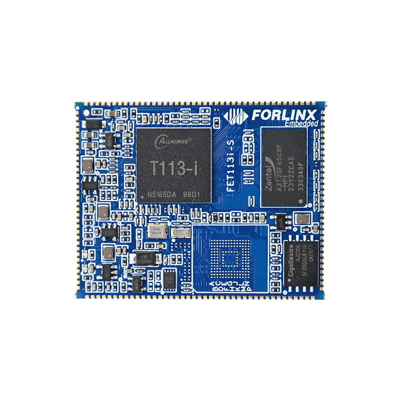
Industrial-grade SoM FET113i-S based on T113-i
FET113i-S SoM is developed and designed based on the T113-i industrial-grade processor released by Allwinner. The T113-i runs at 1.2GHz and integrates a dual-core Cortex-A7 CPU, a 64-bit XuanTie C906 RISC-V CPU, and a DSP to ensure excellent computing power; it not only supports various formats of video decoding and a variety of encoding, but also has a variety of audio interfaces and display interfaces to meet the various needs of multimedia applications. In addition, the T113-i processor has a wide range of connectivity interfaces, including USB, SDIO, UART, SPl, CAN, and Ethernet.
1. Product features:
- Real industrial processor, operating temperature -40 ℃ ~ + 85 ℃;
- Available in 256MB and 512MB memory capacity configuration options;
- With the multi-core heterogeneous architecture of ARM+RISC-V+DSP, it can easily handle various complex scenario requirements;
- Powerful video encoding and decoding capabilities, suitable for various multimedia application scenarios;
- Pre-installed with the 5.4.61 operating system, supports system flashing via TF card and USB OTG.
2. Product appearance and size:
3. Product data list:
- Linux 5.4.61 information, user manual, compilation guide,Linux kernelsource code, file system, factory image, SD flash card making tool, USB OTG flashing tool, Qt test routine source code,Application note*
- Hardware documentation list, including hardware manual, carrier board schematic source files (in AD format), carrier board PCB source files (in AD format), carrier board schematic PDF, chip data sheets, SoM 2D CAD drawing, carrier board 2D CAD drawing, pin no., pin multiplexing table, design guidance*.*: Continuously provide and enrich documentation after product release.
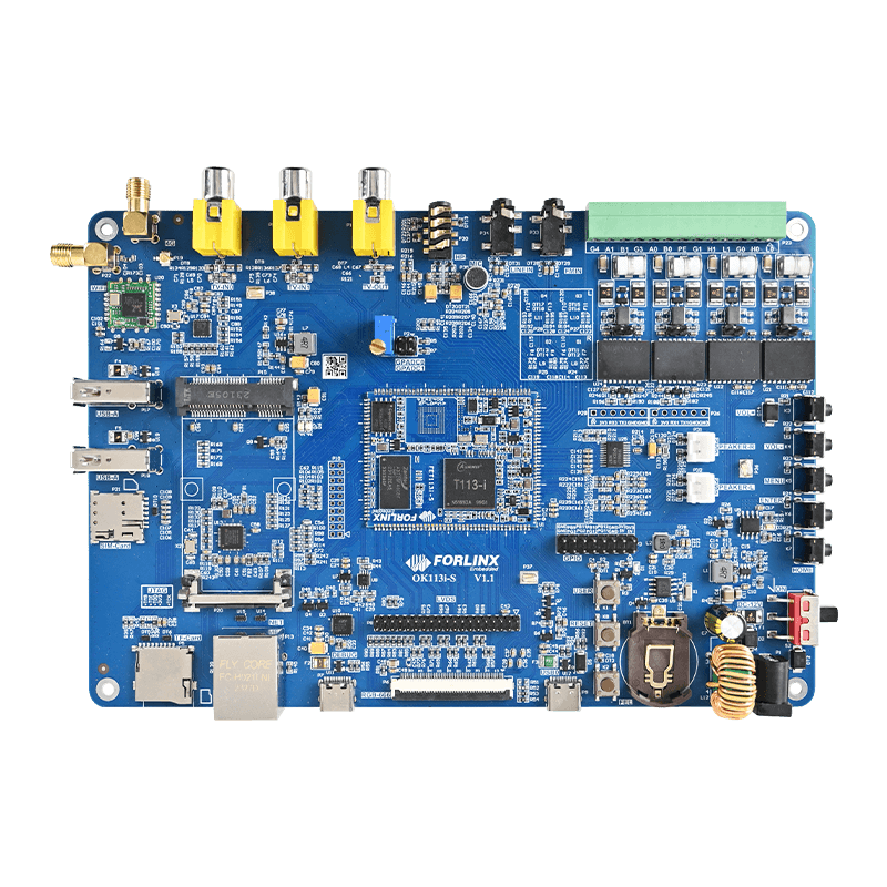
4. OK113i-S Development Board Overall Power Consumption Table
We provide a detailed power consumption test report for your reference. The following is the power consumption table of the whole machine under the Linux system
|
Test Items |
SoM Power(W) |
Development Board Power |
|---|---|---|
| (Including SoM)(W) | ||
| No-load starting peak power | 3.25 | 9.01 |
| No-load standby power | 0.4 | 1.24 |
| CPU stress + memory + eMMC read/write stress test | 1.05 | 1.89 |
| 7-inch LCD screen + 4G + U disk + video decoding | 0.7 | 3.82 |
| 7-inch LCD + 4G + U disk + video encoding | 0.75 | 3.75 |
Note:
1. Test conditions: the SoM configuration is 512MB RAM + 8GB eMMC,4G module Quectel EC20, and the screen is anFolinxoptional product. The SoM is powered by 5V; the carrier board is powered by 12V, and the system is a Linux system.
2. Power consumption is for reference only.
TI13-i SoM Carrier Board Hardware Design Introduction
The FET113i-S SoM features a highly integrated design, with power, resetcircuit, and memory circuits integrated into a compact module. This makes the external circuitry very simple, requiring only a 5V power supply and a reset button to form a minimal system. As shown in the figure below:
Of course, in practical applications, we usually need to connect external devices, such as debugging serial ports and USB interfaces, to perform system flashing and view debugging information. Forlinx provides a detailed default interface definition for the SoM, which allows you to easily add the required functions based on it.
1. Minimum System Schematic
The schematic diagram of the minimum system has been provided and the above diagram is only a schematic for your reference. Note that the source file schematic contains specific connections. To ensure the normal operation of the core board, in addition to the power supply VSYS_5V, it also requires a CPU_RST button, an OTG or SD card interface, and a UART0 debugging serial port circuit. These components not only facilitate system flashing and booting but also facilitate debugging and verifying the operational status of the system.
2. Carrier board Hardware Design Guide
- Power supply requirements
PIN3, PIN4, VCC-5V-SYS Please ensure that the SoM is continuously powered and the current is not less than 1A.
The power supply of PIN2, VCC-3V3 SoM to the carrier board shall not exceed 0.5A, which is only used for timing control and SD card power supply. - Reset Signal
PIN146, CPU-RST-KEY is the reset key interface. Resistor and capacitor loads shall not be added to the carrier board to avoid affecting the normal startup of the SoM. If not in use, it can be left floating. - Electricity levelMatching issues
The PE groups are all 1.8 V levels, so note the level matching. - Signal pins that are not used by the SoM can be left floating, but be sure to connect all GND.
- Power-up sequence
It is strongly recommended that users refer to the design of the development board when designing the carrier board.Please use the VDD_3V3 output from the SoM as the enable for powering up the carrier board and strictly control the power-up timing. Incorrect power-up timing may result in excessive current during the power-up phase, failure of the device to boot, or irreversible damage to the processor. - IO leakage problem
If there is a high level sink current on the signal pin of the SoM, it may cause the SoM to leak electricity. The most typical case is a serial port leakage. In order to avoid this kind of problem, the carrier board adopts the anti-leakage design at the debugging serial port. If the custom-made carrier board also encounters such a situation, it can be handled by referring to development board design.


