Forlinx Development Board丨Support EC20 Hardware Modification Method
At present, many development boards of Forlinx support 4G modules, and the interface is Mini PCIe. The pin definitions and power supply voltages corresponding to the modules of different manufacturers are different. For the support of EC20, the following matters need to be paid attention to on the hardware of each development board:
1. Precautions for Forlinx development board to support EC20 module:
1.1 Mini PCIe pin assignment
As shown in Pic 2, the pin assignments are for the EC20. Among them, pin 30 is UART_DCD (module carrier detection, digital output), and pin 32 is WAKEUP_OUT (module sleep indication, digital output). Figure 3 shows the pin definition of the Mini PCIe socket of the Forlinx development board. In order to be compatible with the standard Mini PCIe interface, pin 30 is set as SMB_CLK (the clock signal of the IIC), and pin 32 is set as SMB_DATA (the data signal of the IIC). When the user designs the baseboard, if the baseboard function supports EC20, the 30 and 32 pins of the Mini PCIe interface of the baseboard cannot be connected to the IIC bus, and need to be left floating, or used as a unique function of EC20.
EC20 powered
1.2.1 3.3V power supply module
The following pic shows the definition of the power interface of EC20: the voltage range is 3.3V ~ 3.6V.
Therefore, users need to meet this power supply range when designing their own baseboard. Please refer to Chapter 2 for the related circuit modification methods that the development board supports EC20.
1.2.2 The development board is compatible with Mini PCIe 1.5V power supply
In order to be compatible with standard Mini PCIe, the development board provides 1.5V power supply to pins 6, 28, and 48. When users design their own baseboards, if they want to support EC20 modules, they need to suspend pins 6, 28, and 48, or use them as the corresponding functions of EC20. Please refer to Chapter 2 for the related circuit modification methods that the development board supports EC20.
2. Forlinx embedded ARM platform modification method
2.1 iMX6 series
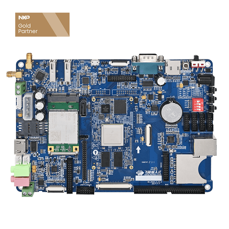
2.1.1 OKMX6Q-C, OKMX6DL-C Development Board
As shown in the figure below, U28, R208, R209, R59, R63, C121, C100, C101, C102 need to be soldered.
2.1.2 OKMX6Q-S3, OKMX6DL-S3 development board
As shown in the figure below, it is necessary to solder U8, R40, R38, R39, C23, C24, C25, and C34 by air, and change R46 from 37.4K to 44.2K_1% precision resistor, that is, adjust the power supply voltage of the 4G module from 3.7V to 3.3V .
2.2 S5P4418/6818 series
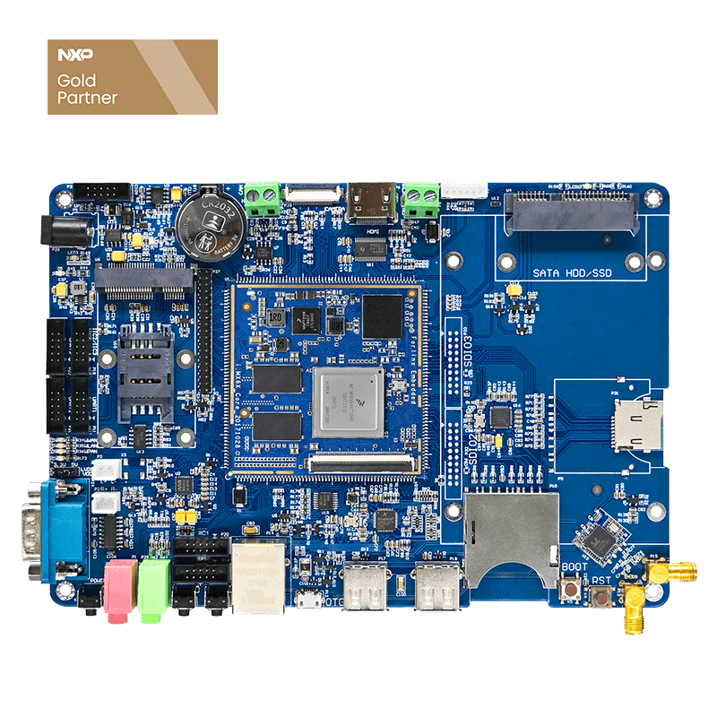
2.2.1 OK4418/6818-C Development Board
As shown in the pic below, it is necessary to air-solder U15, R143, R148, R155, R156, C95, C99, C100, C101, and change R187 to 44.2K_1%, that is, adjust the power supply voltage of the 4G module to 3.3V.
2.2.2 OK4418/6818-C2 development board
As shown in the figure below, it is necessary to air-solder U15, R143, R148, R155, R156, C95, C99, C100, C101, and change R187 to 44.2K_1%, that is, adjust the power supply voltage of the 4G module to 3.3V.
2.3 AM5718 series
2.3.1 OK5718-C
As shown in the pic below, it is necessary to solder U13, R124, R14, R16, C77, C4, C5, and C6 in the air, and change R136 to 44.2K_1%, that is, adjust the power supply voltage of the 4G module to 3.3V.
2.3.2 OK5718-C2
As shown in the pic below, it is necessary to solder U13, R9, R59, R60, C4, C5, C6, and C10 in the air, and change R136 to 44.2K_1%, that is, adjust the power supply voltage of the 4G module to 3.3V.