Introduction to RK3588
What is RK3588?
RK3588 is a universal SoC with ARM architecture, which integrates quad-core Cortex-A76 (large core) and quad-core Cortex-A55(small core). Equipped with G610 MP4 GPU, which can run complex graphics processing smoothly. Embedded 3D GPU makes RK3588 fully compatible with OpenGLES 1.1, 2.0 and 3.2, OpenCL up to 2.2 and Vulkan1.2. A special 2D hardware engine with MMU will maximize display performance and provide smooth operation. And a 6 TOPs NPU empowers various AI scenarios, providing possibilities for local offline AI computing in complex scenarios, complex video stream analysis, and other applications. Built-in a variety of powerful embedded hardware engines, support 8K@60fps H.265 and VP9 decoders, 8K@30fps H.264 decoders and 4K@60fps AV1 decoders; support 8K@30fps H.264 and H.265 encoder, high-quality JPEG encoder/decoder, dedicated image pre-processor and post-processor.
RK3588 also introduces a new generation of fully hardware-based ISP (Image Signal Processor) with a maximum of 48 million pixels, implementing many algorithm accelerators, such as HDR, 3A, LSC, 3DNR, 2DNR, sharpening, dehaze, fisheye correction, gamma Correction, etc., have a wide range of applications in graphics post-processing. RK3588 integrates Rockchip's new generation NPU, which can support INT4/INT8/INT16/FP16 hybrid computing. Its strong compatibility can easily convert network models based on a series of frameworks such as TensorFlow / MXNet / PyTorch / Caffe. RK3588 has a high-performance 4-channel external memory interface (LPDDR4/LPDDR4X/LPDDR5), capable of supporting demanding memory bandwidth.
RK3588 Block Diagram
Advantages of RK3588?
- 1. Computing: RK3588 integrates quad-core Cortex-A76 and quad-core Cortex-A55, G610 MP4 graphics processor, and a separate NEON coprocessor. Integrating the third-generation NPU self-developed by Rockchip, computing power 6TOPS, which can meet the computing power requirements of most artificial intelligence models.
- 2. Vision: support multi-camera input, ISP3.0, high-quality audio;
- 3. Display: support multi-screen display, 8K high-quality, 3D display, etc.;
- 4. Video processing: support 8k video and multiple 4k codecs;
- 5. Communication: support multiple high-speed interfaces such as PCIe2.0 and PCIe3.0, USB3.0, and Gigabit Ethernet;
- 6. Operating system: Android 12 is supported. Linux and Ubuntu will be developed in succession;
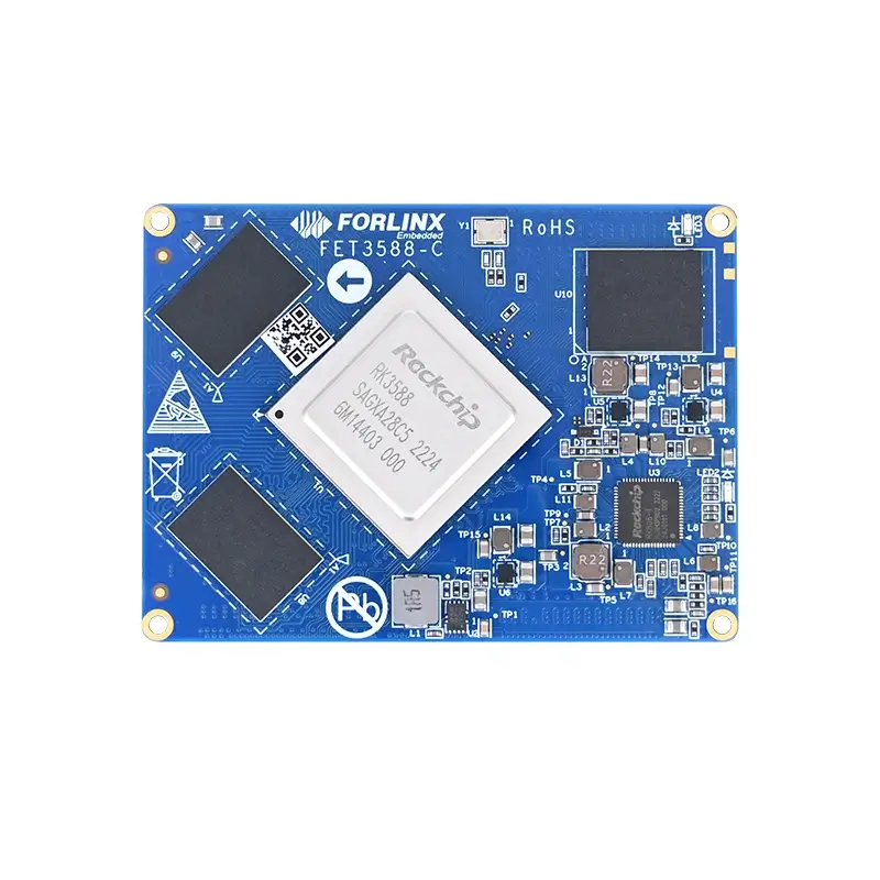
FET3588-C Computer on Module based on Rockchip RK3588
Forlinx FET3588-C SoM inherits all advantages of RK3588. The following introduces it from structure and hardware design.
1. Structure:
- The SoM size is 50mm x 68mm, smaller than most RK3588 SoMs on market;
- 100pin ultra-thin connector is used to connect SoM and carrier board. The combined height of connectors is 1.5mm, which greatly reduces the thickness of SoM; four mounting holes with a diameter of 2.2mm are reserved at the four corners of SoM. The product is used in a vibration environment can install fixing screws to improve the reliability of product connections.
2. Hardware Design:
- FET3568-C SoM uses 12V power supply. A higher power supply voltage can increase the upper limit of power supply and reduce line loss. Ensure that the Forlinx’s SoM can run stably for a long time at full load. The power supply adopts RK single PMIC solution, which supports dynamic frequency modulation.
- FET3568-C SoM uses 4 pieces of 100pin connectors, with a total of 400 pins; all the functions that can be extracted from processor are all extracted, and ground loop pins of high-speed signal are sufficient, and power supply and loop pins are sufficient to ensure signal integrity and power integrity.
- The default memory configuration of FET3568-C SoM supports 4GB/8GB (up to 32GB) LPDDR4/LPDDR4X-4266; default storage configuration supports 32GB/64GB (larger storage is optional) eMMC;
- Each interface signal and power supply of SoM and carrier board have been strictly tested to ensure that the signal quality is good and the power wave is within specified range.
- PCB layout: Forlinx uses top layer-GND-POWER-bottom layer to ensure the continuity and stability of signals.
FET3588-C SoM performance
- • System Frequency
- • Power Supply
- • Working Environment
- • SoM Interface Speed
| Name | Specification | Illustrate | |||
|
|
Minimum | Typical | Maximum | Unit | |
| System frequency ARM Cortex-A76 | - | - | 2400 | MHz | - |
| System frequency ARM Cortex-A55 | - | - | 1800 | MHz | |
| System frequency ARM Cortex-M0 | - | - | - | - | - |
| Parameter | Pin label | Specification | Illustrate | |||
|
|
|
Minimum | Typical | Maximum | Unit | |
| Main Voltage | 12V | 11.5 | 12 | 12.5 | V | - |
| Parameter | Specification | Illustrate | ||||
|
|
|
Minimum | Typical | Maximum | Unit | |
| Operating Temperature | Working Environment | 0 | 25 | 80 | ℃ | Commercial Grade |
| Storage Environment | -40 | 25 | +125 | ℃ | ||
| Humidity | Working Environment | 10 | - | 90 | %RH | No Condensation |
| Storage Environment | 5 | - | 95 | %RH | ||
| Parameter | Specification | Illustrate | |||
|
|
Minimum | Typical | Maximum | Unit | |
| Serial Communication | - | 115200 | 4M | bps | - |
| SPI Clock Frequency | - | - | 50 | MHz | - |
| I2C Communication | - | 100 | 400 | Kbps | - |
| USB3.0 Interface | - | - | 5 | Gbps | - |
| USB2.0 Interface | - | - | 480 | Mbps | - |
| CAN Communication | - | - | 1 | Mbps | - |
| PCIe2.1 | - | - | 5 | Gbps | - |
| PCIe3.0 | - | - | 8 | Gbps | - |
OK3588-C Development Board (Android) Power Consumption Table
Peak Current
| Hardware | Test Items | Supply Voltage (V) | Working Current (mA) | |
|
|
|
|
Peak Current | Stable Value |
| Development board | Standby power consumption | 12 | 700 | 280 |
| SoM only | Standby power consumption | 12 | 480 | 91 |
| Run points | 12 | 550 | 480 | |
Note:
1. Peak current: the maximum current value during startup;
2. Stable value: the current value when it stays on the startup interface after starting.
RK3588 SoM hardware design Guide
FET3588-C SoM has integrated power supply and storage circuit in a small module. The required external circuit is very simple. A minimal system only needs power supply and startup configuration to run, as shown in the figure below:
The minimum system includes SoM power supply, system flashing circuit, and debugging serial port circuit. The minimum system schematic diagram can be found in "OK3588-C_Hardware Manual". However, in general, it is recommended to connect some external devices, such as debugging serial port, otherwise user cannot judge whether system is started. After completing these, on this basis, add the functions required by user according to default interface definition of RK3588 SoM provided by Forlinx.
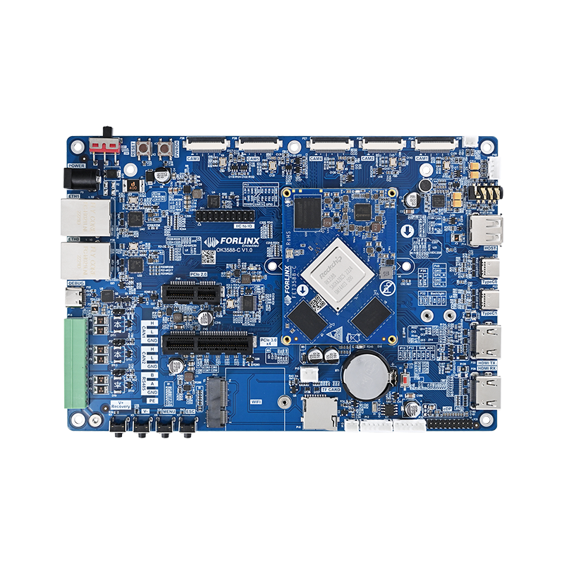
RK3588 Carrier Board Hardware Design Guide
The interface resources derived from Forlinx embedded OK3588-C development board are very rich, which provides great convenience for customers' development and testing. Moreover, OK3588-C development board has passed rigorous tests and can provide stable performance support for customers' high-end applications.
In order to facilitate user's secondary development, Forlinx provides RK3588 hardware design guidelines to annotate the problems that may be encountered during design process of RK3588. We want to help users make the research and development process simpler and more efficient, and make customers' products smarter and more stable. Due to the large amount of content, only a few guidelines for interface design are listed here. For details, you can contact us online to obtain "OK3588-C_Hardware Manual" (Click to Inquiry)
• Carrier board power supply
1. When customer designs it by himself, it is necessary to ensure power-on sequence of power supply;
2. The components selection and external layout of buck-boost chip need to refer to the corresponding chip manual to ensure a good power circuit.
• DEBUG
1. In order to facilitate later debugging, please lead out debugging serial port when designing carrier board by yourself;
2. It is recommended to keep Q1 and Q2, which can effectively prevent the current of U5 from flowing back into CPU through UART2_TX/RX when SoM is not powered on, which will affect the startup and even cause damage.
• TF Card
1. TF card power supply needs to be controlled, refer to carrier board circuit;
2. Impedance requirements: single-ended 50ohm;
• SATA3.0 Circuit
1. During Slot design, the peripheral circuit and power supply need to meet Spec requirements;
2. 10nF AC coupling capacitors connected in series on TXP/N and RXP/N differential signals of SATA interface, AC coupling capacitors are recommended to use 0201 package, lower ESR and ESL, and can also reduce impedance changes on line;
3. All signals of eSATA interface socket must be added with ESD, placed close to socket during layout, and ESD parasitic capacitance shall not exceed 0.4pF;
• Ethernet circuit
1. In RGMII mode, TX/RX clock path inside RK3588 integrates delayline, which supports adjustment; the default configuration of reference figure:
The timing between TXCLK and data is controlled by MAC.
The timing between RXCLK and data is controlled by PHY (for example, use RTL8211F/FI,
2nS delay is enabled by RXCLK default. Other PHYs should pay attention to this configuration);
2. GMAC0 interface level only supports 1.8V. GMAC1 interface level defaults to 3.3V (if you must change it to 1.8V, please contact Forlinx), you need to pay attention to whether the power supply voltage of PHY chip RGMII signal power domain is the same as GMACx interface level match;
3. The Reset signal of Ethernet PHY needs to be controlled by GPIO. The level of GPIO must match the level of PHY IO. A 100nF capacitor must be added near PHY pin to enhance antistatic ability. Note: the reset pin of RTL8211F/FI only supports 3.3V level;
4. TXD0-TXD3, TXCLK, TXEN need to reserve 0ohm resistors in series at FET3588, and improve the signal quality conditionally according to actual situation;
5. RXD0-RXD3, RXCLK, RXDV need to be connected in series with 22ohm resistors at PHY to improve signal quality;
6. When PHY uses an external crystal, please select crystal capacitor according to the load capacitance value of crystal actually used, and control the frequency deviation at ±20ppm;
7. The RSET pin of RTL8211F/FI has an external resistance of 2.49K ohm and an accuracy of 1%, which cannot be modified at will;
8. MDIO must be externally added with a pull-up resistor, 1.5-1.8Kohm is recommended, and the pull-up power supply must be consistent with IO power supply;
9. PCB Layout needs to ensure the integrity of RGMII signal reference plane, and the integrity of the peripheral power reference plane of PHY chip;
10. Equal length requirements: The receiving and sending of RGMII can be grouped into equal lengths, and the equal length requirement is ≤12.5mil;
11. Impedance requirements: single-ended 50ohm;
Only a few points for attention in the design of RK3588 carrier board are listed here. Forlinx Embedded provides rich and complete development documents and tools for RK3588 SoM, including RK3588 schematic diagrams, common tools, and software source code, development environment, test routines, chip data sheets, etc. In order to facilitate the secondary development of RK3588 for users, Forlinx Embedded has also prepared a wealth of use materials, including software manual, hardware manual, compilation manual, application notes, common QA question and answer manuals, pin multiplexing and pin function comparisons table etc. You can contact Forlinx Embedded Online to get it ( click to inquiry)
Application
RK3588 has a wide range of application directions, and can be used in information release terminal, smart cockpit, smart large screen, AR/VR, edge computing, high-end IPC smart NVR, high-end tablet, ARM PC, visual gateways, and many other product applications.