Hardware Design Instructions of iMX6ULL SoM
NXP i.MX6ULL extends the i.MX6 family. It is a high-performance, ultra-efficient, low-cost processor. It features an advanced ARM Cortex-A7@800MHz. The i.MX6ULL includes an integrated power management module that reduces the complexity of external power supplies and simplifies power-up sequencing. Target Application: Automotive telematics, IoT Gateway, HMI, Home energy management system, Smart Energy Information Concentrator, Intelligent industrial control system, POS, Portable medical equipment, Printers and 2D scanners…
Block Diagram of i.MX6ULL Processor
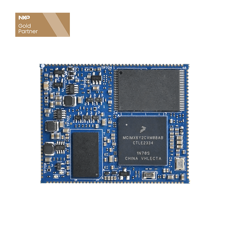
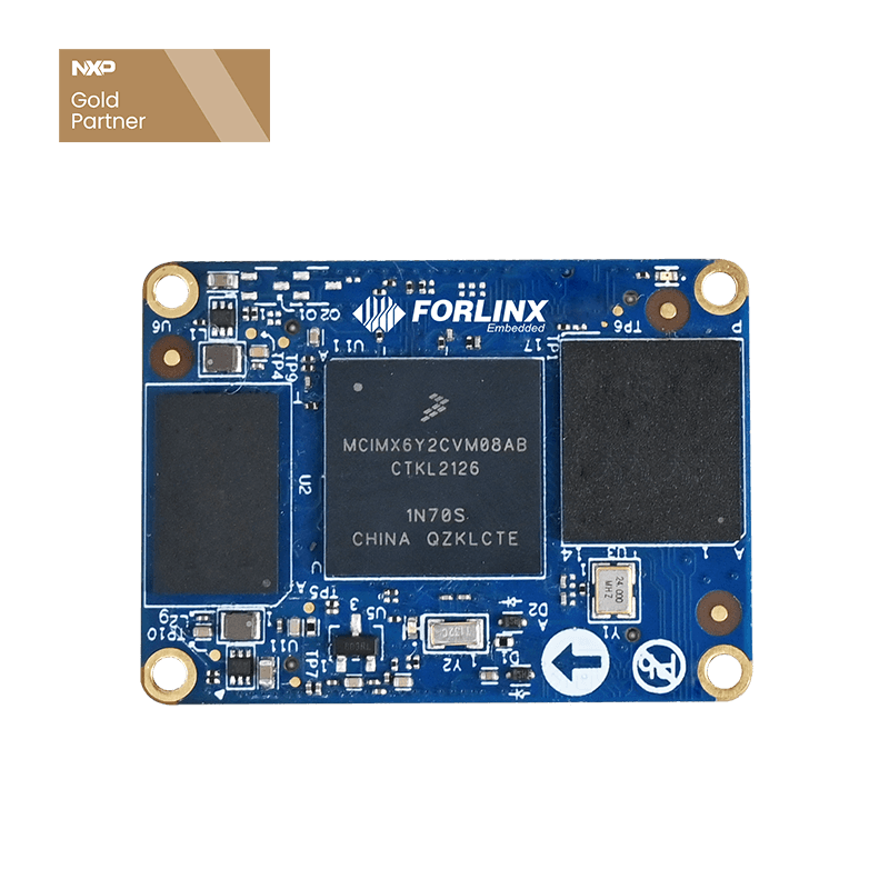
FETMX6ULL-C system on module(SoM) is Forlinx latest product, which is based on NXP Cortex-A7 low power featuring processor i.MX6ULL@ 800MHz. Native support: 8 serial ports, 2 Ethernet ports, 2 CAN controller, 2 USB 2.0, LCD…Ultra-Small size design, only 40*29mm, suitable for application scenarios with a limited volume.
Linux system power consumption measurement table of FETMX6ULL-C SoM
| Item | Test | Power Supply(V) | Peak Current(mA) | Constant Current(mA) |
| 1 | No screen + no operation | 5±5% | - | 250 |
| 2 | Loaded 4.3 inch screen + no operation | 5±5% | - | 315 |
| 3 | Loaded 7-inch screen + no operation | 5±5% | - | 587 |
| 4 | Loaded 4.3-inch screen + video playback + 100% CPU usage | 5±5% | 360 | 340 |
| 5 | Loaded 7-inch screen + video playback + 100% CPU usage | 5±5% | 715 | 700 |
Note:
Peak current: the maximum current value during startup;
Constant current: The current value when it stays on the interface after startup.
Hardware Design Instruction
FETMX6ULL-C SOM has integrated power supply, reset monitoring circuit, and storage circuit. The required external circuit is very simple. It only needs 5V power supply, reset key, and startup configuration to form a minimum system, as shown in the following figure:
Schematic diagram of minimal system design based on FETMX6ULL-C SoM
Note:
When user designs carrier board, the serial port circuit must be reserved for debugging.
When user designs carrier board, the DIP switch circuit must be reserved for program flashing.
User should pay attention to the power-on sequence when designing carrier board to prevent the occurrence of latch-up from damaging the CPU (refer to 3.5.1 Power Supply of Carrier Board for specific design).
Besides, it is recommended to connect some external devices, such as debugging serial port...otherwise, user cannot judge whether system is started. After this, user can add required functions according to the default interface definition of SOM by Forlinx. For PIN definitions of iMX6ULL series SoM, please contact Forlinx sales.
Hardware Design Guidelines
1. Boot configuration
i.MX6ULL supports multiple flashing and booting methods. After system is powered on or reset, it selects different programming and booting methods, by reading the state of system boot configuration pin.
User must add this circuit when designing carrier board, For the specific configuration method, please refer to schematic diagram of carrier board and the boot configuration chapter of Forlinx hardware manual. Meanwhile, user must add control to LCD_DATA11, if needs SD card flashing and eMMC booting at the same time. Otherwise, user can set LCD_DATA11 fixed level as needed.
2. PMIC_ON_REQ drive capability
GEN_5V and GEN_3.3V on carrier board are obtained by the control of PMIC_ON_REQ. The current drive capability of PMIC_ON_REQ is too weak, and a voltage-controlled switching element needs to be used. The N-channel field effect transistor AO3416 is used in the development board. Please refer to power circuit design of carrier board.
3. IIC bus adds pull-up resistor
When user designs the carrier board, IIC bus must be added with a pull-up resistor, otherwise IIC bus devices may not work. Currently, the 2 IIC buses drawn from carrier board are both pulled up to 3.3V through 1.5K resistors.
4. During debugging, encounter error USB1-1
When use the USB interface, user need to connect USB_OTG1_VBUS and USB_OTG2_VBUS to 5V, otherwise it will encounter error USB1-1. Currently, on carrier board, USB_OTG2_VBUS is connected to GEN_5V through a 0Ω resistor.
5. RX pin output level of CAN circuit
The CAN transceiver chip currently used by OKMX6ULL-C SBC is TJA1040T by default. The RX output level of the chip is 5V, while the level of this pin of CPU is 3.3V. In order not to affect the 3.3V power supply inside the CPU, it is necessary to divide the voltage with series resistor to ground on the RX of chip, and then connect to the CPU. Please refer to the circuit of CAN.
6. The pins not used by user design should be left floating.