How to Configure i.MX6ULL GPIO?
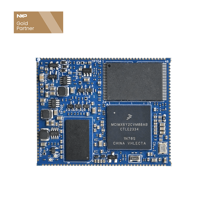
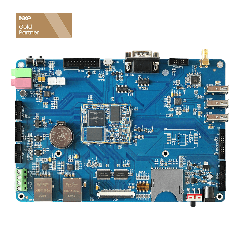
This article is based on OKMX6ULL-S development board of Forlinx embedded. Reference only for other i.MX6ULL development board
GPIO configuration of i.MX6ULL
i.MX6ULL runs Linux. In Linux, there is a file dedicated to configuring various peripherals of processor, including GPIO. This file is "device tree". The path of i.MX6ULL device tree in kernel source code: arch/arm/ boot/dtbs/
Many device tree files are in this path. The device tree here to use are okmx6ull-s-emmc.dts and okmx6ull-s-nand.dts. Open any of the device tree files, it can be seen both refer to imx6ull-14x14-evk.dts. So the modifications to device tree are based on imx6ull-14x14-evk.dts.
Find &iomuxc node, we can see some GPIOs have been multiplexed under pinctrl_hog_1:hoggrp-1 node, as follows:
1. Hardware schematic analysis
View hardware schematic diagram. There are two LED on OKMX6ULL carrier board. Take LED2 as an example. The cathode of LED2 is connected to GPIO9. When GPIO9 is low, LED lights up.
Open hardware material/user manual/FETMX6ULx-S SoM pin function assignment table, and find out GPIO9 corresponds to GPIO1_IO09 of i.MX6ULL.
2. Set pin multiplexing
As mentioned earlier, pin multiplexing is added under &iomuxc node. Set parameter to 0x17059 first, and the configuration method will be explained later. The configuration is as follows:
3. Comment out conflicting part
Next, open arch/arm/boot/dts/imx6ull-14x14-evk.dts in kernel source code.
To prevent this node from affecting GPIO modification, first it needs to comment out LED node in device tree, as shown in red box of following figure:
4. update device tree
Recompile device tree with following command:
/opt/fsl-imx-x11/4.1.15-2.0.0/environment-setup-cortexa7hf-neon-poky-linux-gnueabi //Execution environment variables
make dtbs will compile all device trees. After compiling, check again to confirm a new dtb file has been generated.
Next, copy the device tree file just generated to OKMX6ULL-S development board. You can copy by USB flash disk, or network services such as TFTP, NFS, and FTP.
Taking eMMC version as an example, you can directly copy device tree file: okmx6ull-s-emmc.dtb to /run/media/mmcblk1p1/, replace the file with same name in the path, and then restart development board.
5. Modify GPIO
5.1. Calculate the value corresponding to sys/class/, gpio GPIOn_IOx= (n-1)*32 + x
GPIO1_IO09=(1- 1)*32 + 9 = 9
5.2 Set GPIO1_IO09= as output
echo9 > /sys/class/gpio/export: GPIO pin number used to notify system control needs to be exported
echo"out" > /sys/class/gpio/gpio9/direction: control as output
echo"1" > /sys/class/gpio/gpio9/value: output is high and LED is off
Or echo"0" > /sys/class/gpio/gpio9/value: output is low, LED is on
echo9 > /sys/class/gpio/unexport: notify system to cancel export
6.GPIO parameters illustration
The long string of MX6UL_PAD_GPIO1_IO09__GPIO1_IO09 is a macro definition, which can be viewed in imx6ul-pinfunc.h. You may have noticed that imx6ul-pinfunc.h file is 6UL. Because imx6ull-pinfunc.h references imx6ul-pinfunc.h, and added some content.
Open arch/arm/boot/dtbs/imx6ul-pinfunc.h and find the macro definition of MX6UL_PAD_GPIO1_IO09 as follows:
These macro definitions are functions GPIO1_IO09 can be multiplexed. There are 5 parameters behind each macro definition, plus 0x17059 just configured under &iomuxc node, a total of 6 parameters. GPIO configuration can be completed with them. The 6 parameters are:
mux_ctrl_ofs: MUX register offset address
pad_ctrl_ofs: PAD register offset address
sel_input_ofs: Input select register offset address
mux_mode: MUX register value
sel_input: input select register value
pad_ctrl: PAD register value
Above 6 parameters correspond to offset address and register value of 3 registers.
1. MUX register
The full name is SW_MUX_CTL_PAD_GPIO1_IO09, which means GPIO multiplexing register. You can find detailed introduction in i.MX6ULL data sheet from hardware material/data sheet/i.MX6ULLRM.pdf by Forlinx.
Open section 32.6.16, you can see the register offset address is consistent with the file provided by Forlinx. ALT0-ALT8 corresponds to functions this GPIO can be multiplexed, and 0x5 corresponds to multiplexing GPIO5_IO09 into GPIO1_IO09.
2. PAD register
The full name is SW_PAD_CTL_PAD_GPIO1_IO09, which means GPIO electrical parameter configuration register. You may pay attention to it. Because NXP has already written macro definitions for MUX register and input selection register. But value of this register needs to be set by user according to his own needs. The reference material is still i.MX6ULLRM.pdf in section 32.6.162. There is a detailed explanation about each bit of PAD register.
HYS (bit16): enable hysteresis comparator, which is valid when IO is used as input. Turning on hysteresis comparator can filter out some interference. When this bit is 0, hysteresis comparator is disabled, while 1 is enabled.
PUS(bit15:14): Set pull-up or pull-down resistor, there are four options:
PUE(bit13): When IO is used as input, this bit is used to set IO to use pull-down or state holder. When 0, state holder is used, and when 1, pull-up or pull-down is used. State holder is only available when IO is used as input. This IO port can maintain the previous state when external circuit is powered off.
PKE(bit12): This bit is used to enable or disable pull-up or pull-down/state holder. When 0, pull-up or pull-down/state holder is disabled, while 1, pull-up or pull-down/state holder are enabled.
ODE(bit11): Open-drain enable. When IO is used as output, it is used to disable or enable open-drain output. When 0, open-drain output is disabled, while 1, open-drain output is enabled. .
SPEED(bit7:6): When IO is used as output, this bit is used to set IO speed.
DSE (bit5:3): When IO is used as output, it is used to set driving capability of IO. It can be understood as the size of resistor connected in series on IO port. The smaller resistance, the stronger driving capability. There are 8 options in total:
SRE(bit0): IO flip speed. When 1, IO level transition time is faster, and the corresponding waveform is steeper; when 0, IO level transition time is slower and waveform is smoother.
After introducing each bit of PAD register, take a look at 0x17059 just configured, and expand it into binary: 0001 0111 0000 0101 1001.
Bit15:14 is set to 01, which corresponds to 100K pull-up. This is because the cathode of LED is connected to GPIO, and LED is off by default.
Bit5:3, the configuration here is R0/6, you can also try to configure it to other values, and observe whether the brightness of LED will change.