G2L Series SoM - RZ/G2L Overview
RZ/G2L is a high-performance, ultra-efficient processor for intelligent industrial control from Renesas, ARM [email protected], integrated with ARM Cortex-M33@200MHz, and Mali-G31 GPU@500MHz. Supports a variety of display interfaces and rich industry application interfaces. Suitable for industrial control with video output.
Target applications are industrial HMI, smart thermostat, home appliance, walkie-talkie/doorbell, POS terminal, home security camera, barcode scanner, industrial gateway, etc.
RZ/G2L block diagram
To help engineers learn this stable and easy-to-use processor, and develop product with it more convenient and fast, Forlinx, a leading embedded ARM board manufacturer in China, has a strong cooperation with Renesas Electronics, launched SoM FET-G2LD-C based on RZ/G2L.
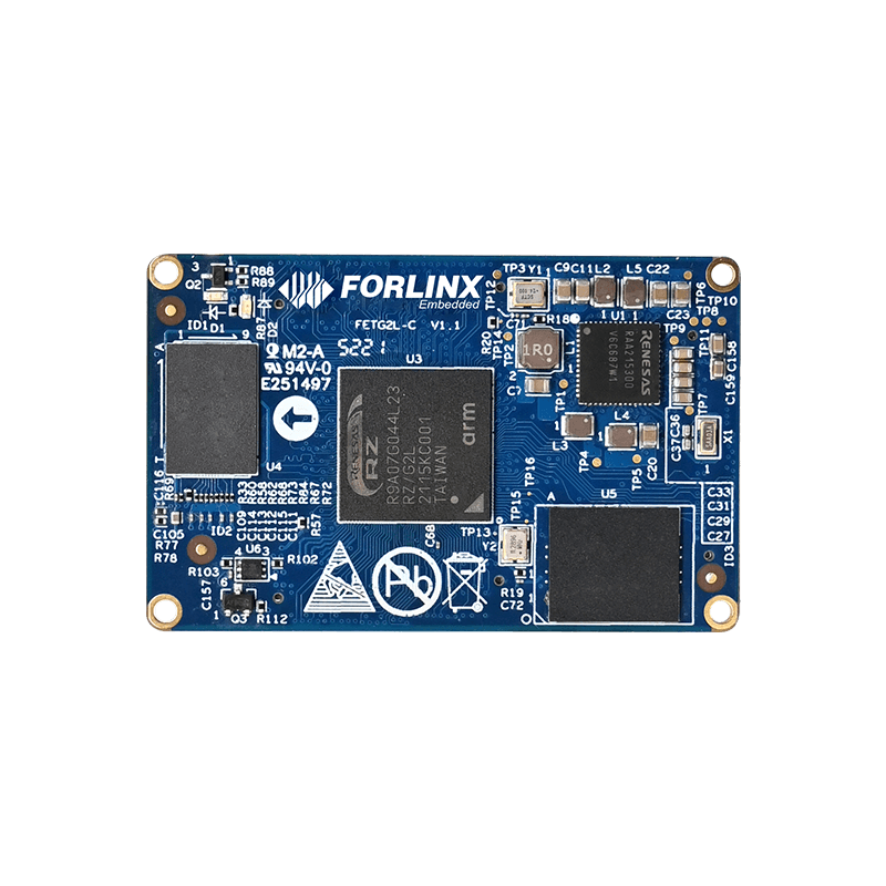
1. What is FET-G2LD-C Core Board?
Core board FET-G2LD-C carries Cortex-A55+Cortex-M33 heterogeneous processor RZ/G2L. Rich interface resources 2x 1000Mbps Ethernet (GMAC), 2x CAN-FD, 7x UART, USB 2.0, SPI, IIC, MTU , ADC, etc.. With Multi-function timer pulse unit, supports Toggle, PWM, complementary PWM and reset synchronous PWM modes, supports dead time compensation counter function. Multiple display interfaces MIPI-DSI, RGB, up to 1920x1080. Onboard QSPI Flash, separate storage of uboot, more stable. Safe and reliable from Renesas’ technical accumulation of Automotive Electronics. 10 years + supply cycle, bulk supply is guaranteed.
With the integrated power supply solution, the SoM size is very small, only 60mm x 38mm. With ultra-thin board-to-board connectors, the highest part (inductor) of SoM is only 5.6mm away from the surface of carrier board, applicable to products with limited space(Because the connector has two versions of 2mm height and 2.5mm height, 2mm height connector is used by default). The SoM production technology takes immersion gold and resin plug holes, which significantly enhanced the reliability and stability of welding. And its materials are lead-free, complies with environmental requirements. Meanwhile, the signal integrity and power integrity are strictly handled, provide a theoretical basis for the stable operation of the system by simulation. The four corners of SoM reserve fixed holes to cope with high-intensity vibration scenarios.
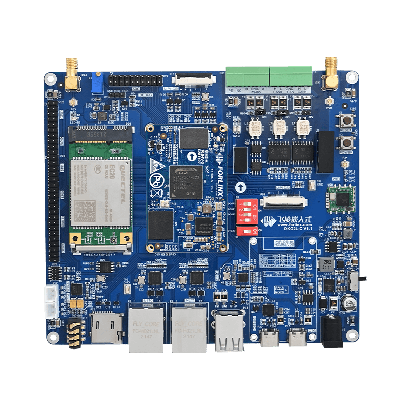
2. OKG2LD-C Development Board
SBC OKG2LD-C is the evaluation kit of the FET-G2LD-C core board. It has rich common interfaces, and adds EMC protection reference design for RS485, CAN. Help users develop products easily, lower difficulty, and reduce work.
3. RZ/G2L Series Power Consumption Measurement Table(Linux System)
Note:
Peak current: the maximum current value during startup
Constant current: The current value when it stays on the interface after startup.
4. SoM based on RZ/G2L Hardware Design Guideline
SoM FET-G2LD-C has integrated power supply and storage circuit into one module. The required external circuit is very simple. Just needs power supply and startup configuration to run, as shown in the following figure:
However, it is recommended to connect some external devices except the minimum system, such as debugging serial port. Otherwise the user cannot judge whether the system is started. After this, add the functions required by users according to the default interface definition of SoM FET-G2LD-C by Forlinx.
For the pin definition details, please contact Forlinx.
(1) Minimal system schematic diagram of SoM based on G2L
Note: The minimum system includes SoM power supply, system flashing circuit, and debugging serial port circuit. For other peripheral circuit designs of RZ/G2L core board, please contact Forlinx.
(2) Hardware design guideline of RZ/G2L series carrier board
Power Supply:
The following power-on sequences need to be strictly observed:
The input voltage is converted into 5V by DCDC chip to supply power to SoM. The Power Good signal of DCDC chip is the enable signal (VIN_PWR_BAD#) of SoM PMIC. The Power Good signal of SoM PMIC is the enable signal ( PMIC_PGOOD) of other power supplies on carrier board.
The PMIC_PGOOD output by SoM RZ/G2L is an open-drain output, and there is a pull-up resistor on SoM. PMIC_PGOOD is a 10K pull-up on SoM. When performing timing control, please pay attention to divide voltage of pull-down resistor. If necessary, logic gates can be added to avoid voltage division issue.
Check whether the power-on sequence meets the requirements, and whether there is a problem of current backflow caused by RZ/G2 carrier board or peripherals being powered on first. If it has such problem, it needs to add an anti-current backflow circuit such as a buffer chip on RZ/G2 carrier board.
It is recommended to add test points or indicators for each power supply to facilitate board debugging.
Check weather the power network name for each device is correct.
Check whether the routing of each power supply can meet the current requirements.
Check whether the voltage design of each power supply is correct.
Check whether the DCDC circuit layout meets the requirements of the corresponding chip manual. It is necessary to ensure that the high-frequency circuit is the minimum return path.
Boot-up:
Check whether boot circuit meets the boot requirements, and whether BOOT configuration can correspond to the required boot medium.
It is recommended to reserve RESET key.
Check whether the design of RZ/G2 carrier board reserves a debug interface (debugging serial port).
Check whether the design of RZ/G2 carrier board reserves a flashing interface (such as SD interface, etc.).
Interfaces:
Check whether there is a corresponding pull-up resistor on IIC bus;
Check whether the sampling voltage range of ADC input interface is 0~1.8V;
Check whether the levels match of each bus, like IIC, SPI;
Check whether MIPI CSI isometric, impedance, etc. meet the requirements;
Check whether MIPI DSI isometric, impedance, etc. meet the requirements;
Check whether USB0_VBUSEN and USB1_VBUSEN directly drive the power switch chip, or add related gate circuits;
USB0_OVRCUR and USB1_OVRCUR need to be connected to OC of USB power switch chip. If OVRCUR function is not used, these two pins need to be pulled up to 3.3V by a pull-up resistor;
To unify the interface, Forlinx G2L series development board uses Type-C socket. Therefore, the DIP switch is used to select USB0_OTG_ID level to identify master/slave device. Users can use other interfaces when designing their own carrier boards;
SD card power supply needs to be controlled. Otherwise the card may not be recognized after system reset;
Pay attention that RGMII interface level is 1.8V, and PHY chip should be configured with corresponding registers and peripheral circuits to ensure level matching;
Check whether the network PHY chip is correctly connected to MDC and MDIO buses;
Check whether the PHY address of Ethernet PHY chip conflicts;
(3) RZ/G2L series user profile
Forlinx provides rich development materials for RZ / G2L series SoM and SBC.
Linux4.19 includes:
User Manual, Compilation Instruction Manual, Linux Kernel Source Code, File System, Factory Image, Development Environment VM Ubuntu Image, SD Flash Card Making Tool, USB OTG Flash Tool, QT Test Routine Source Code, Application Notes*, Development Environment Docker Deployment package*.
Hardware includes:
Hardware manual, carrier board schematic source file (AD format), carrier board PCB source file (AD format), carrier board schematic PDF, chip data manual, SoM 2D CAD drawing, carrier board 2D CAD drawing, pin function multiplexing table*, Design Guidance*.
*: After the product is released, provide and enrich the materials one after another