Forlinx RZ/G2L System on Module and SBC Evaluation
In mid-May 2022, Forlinx released FET-G2LD-C SoM and OK-G2LD-C SBC based on Renesas RZ/G2L, which has rich peripheral interfaces, high performance with low power consumption.
Renesas RZ/G2L was launched in 2021. Some engineers don’t know it very well and have many questions about it. The following is product test of FET-G2LD-C SoM and OK-G2LD-C SBC for some FAQs.
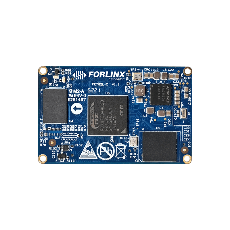
FET-G2LD-C System on Module(SoM)
- CPU: RZ/G2L
- Dual-Core Arm® Cortex®-A55 @ 1.2GHz
- Single Core Arm® Cortex®-M33 @ 200MHz
- GPU: Arm® MaliTM-G31 @ 500MHz
- Memory: DDR4-1600 (current version is 2GB)
- Storage: eMMC (16GB) + QSPI Flash (16MB)
- Power supply: integrated power chip
- Package: ultra-thin board to board connector
FET-G2LD-C SoM carries high-performance and ultra-efficient processor Renesas RZ/G2L. It’s heterogeneous multi-core, Cortex-A55, 1.2GHz, and integrates a MCU Cortex-M33, 200MHz. FET-G2LD-C SoM has a GPU Mali-G31 500MHz and supports a variety of display interfaces. It has rich functional interface resources, like multi-channel UART, Ethernet, CAN-FD, etc. It is applicable to industrial, medical, electric power, transportation and other pan-industrial application scenarios.
FET-G2LD-C SoM front and back
FET-G2LD-C SoM Front and Back Dimensions
With the integrated power supply solution, the SoM size is very small, only 60mm x 38mm. With ultra-thin board-to-board connectors, the highest part (inductor) of SoM is only 5.6mm away from the surface of carrier board, applicable to products with limited space. The SoM production technology takes immersion gold and resin plug holes, which significantly enhanced the reliability and stability of welding. And its materials are lead-free, comply with environmental requirements. Meanwhile, the signal integrity and power integrity are strictly controlled. Through simulation, provide a theoretical basis for the stable operation of the system. The four corners of SoM reserve fixed holes to cope with high-intensity vibration scenarios. In addition, it has fool-proof design.
2. RZ/G2L SoM stability test
1) Power stability test:
For the stability of power supply, Forlinx tested SoM under full load, and captured the waveform of each test point by oscilloscope:
SoM TP1 waveform
SoM TP2 waveform
SoM TP3 waveform
SoM TP4 waveform
SoM TP5 waveform
SoM TP6 waveform
SoM TP7 waveform
SoM TP8 waveform
SoM TP9 waveform
SoM TP10 waveform
3. Memory stress test:
The memory stress test results of FET-G2LD-C SoM are shown in the figure below.
Results of memory stress test
It can be seen FET-G2LD-C SoM performed very well in the full load stress test.
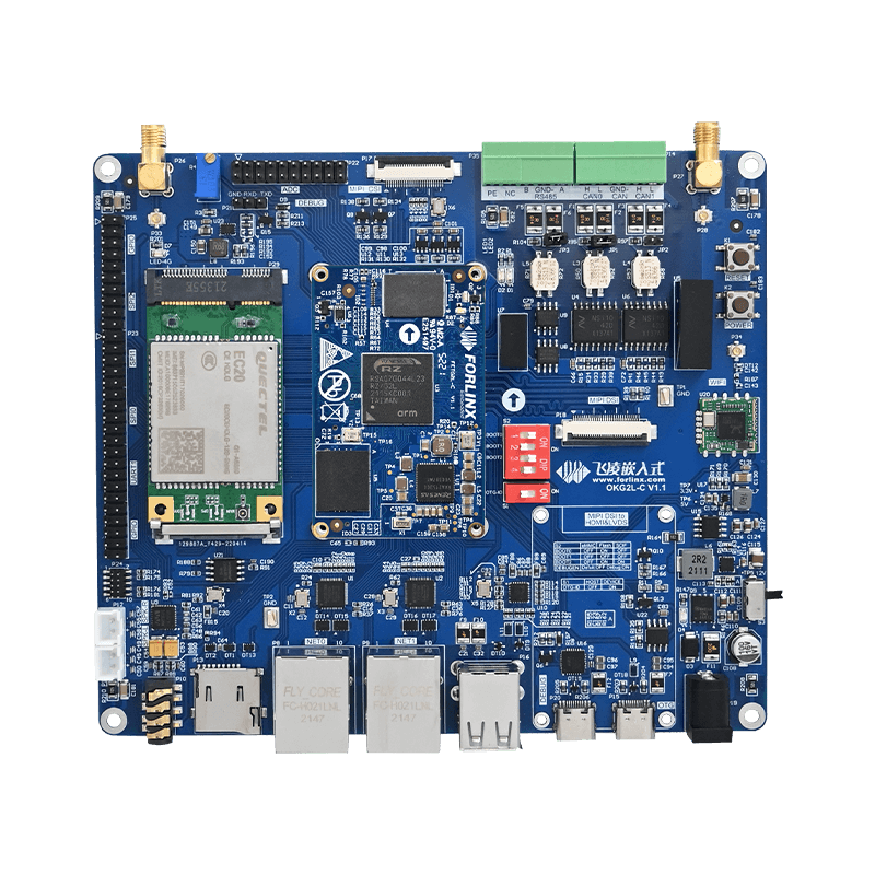
4. OK-G2LD-C Single Board Computer
The carrier board layout of Forlinx OK-G2LD-C SBC is compact, size only 150mm x 130mm. However the interfaces are very rich, like two Gigabit Ethernet, two USB2.0, USB OTG, TF, two CAN-FD, RS485, MIPI-CSI, MIPI-DSI, headphone output, speaker output, MIC input, ADC... onboard WIFI&BT module, reserved MIPI PCIe slot for 4G module.
The peripheral interfaces have corresponding protection circuit, and each interface is close to the board edge, which is convenient for users to make their own shells or place it in the chassis.
Carrier Board Dimensions
1) power consumption test
Many clients are concerned about the power consumption of FET-G2LD-C SoM and OK-G2LD-C SBC. Therefore, Forlinx has tested them respectively. The result is shown below:
When the SoM is fully loaded, the power consumption is only 1.8w. With the low power consumption, FET-G2LD-C SoM can be designed without fan or heat sink if working environment with good air flow. (if it is Hermetic environment, it needs to be evaluated based on practice)
2) Development board startup test
OK-G2LD-C SBC supports TF card flash, SCIF and Flash startup (eMMC startup is not available now). The silk screen next to dial switch on carrier board is the position of dial code in different states. User can dial directly according to the silk screen. As shown in the figure below, the DIP switch is Flash startup:
Our SoM and development board based on Renesas RZ/G2L are hot selling now. Please inquiry Forlinx for details.