


FET536-UP4 System on Module
CPU: Allwinner T536
Architecture: 4x [email protected]+RISC-V@600MHz
Frequency: 1.6GHZ
RAM: 1GB/2GB/4GB LPDDR4
ROM: 8GB/16GB/32GB eMMC
System: Linux 5.10
Forlinx FET536-UP4 SoM: Allwinner T536 Industrial Edge AI System-on-Module
The FET536-UP4 System-on-Module (SoM) is engineered around the Allwinner T536 industrial-grade processor. Featuring a multi-core heterogeneous architecture, it integrates a quad-core ARM Cortex-A55 processor (up to 1.6 GHz) and a 64-bit XuanTie E907 RISC-V MCU to deliver highly efficient computing power. Built for high-reliability edge applications, it incorporates a 2 TOPS Neural Processing Unit (NPU), secure boot, national cryptographic algorithm support, full-path ECC, and Asymmetric Multi-Processing (AMP) running on Linux-RT. Utilizing strictly industrial-grade components, this cost-effective module is optimized for demanding deployment fields such as data concentrators, FTU, DTU, EV charging stations, transportation, robotics, and industrial control .
Highlights:
- Heterogeneous Compute & AI: ARM Cortex-A55 + RISC-V MCU multi-core architecture paired with a 2 TOPS NPU suitable for diverse edge scenario requirements.
- Industrial Reliability: Features full-path ECC, secure boot, national cryptographic support, and AMP real-time control on Linux-RT.
- Extensive Connectivity: Equipped with 4x CAN-FD, 17x UART, Ethernet, USB, SDIO, SPI, ADC, and a high-speed parallel LocalBus.
- Scalable Configurations: Rich product configurations available with 1GB, 2GB, or 4GB options to optimize cost reduction across key deployment fields.
- Compact & Universal Design: Integrates an LCC+LGA package and maintains seamless pin-compatibility with the broader UP4 series of SoMs.
FET536-UP4 SoM
Powered by the Allwinner T536 industrial processor, the FET536-UP4 is a cost-effective System on Module featuring an ARM+RISC-V heterogeneous architecture,
2 TOPS NPU, full-path ECC memory protection, and rich I/O (17× UART / 4× CAN-FD)
delivering a highly reliable edge computing solution for FTU/DTU, EV charging stations, and industrial control systems.
What is the UP4 Package?
UP4 is a standardized System-on-Module (SoM) footprint defined by Forlinx Embedded.
"UP" stands for Universal Package, and "4" indicates its 40mm × 40mm physical form factor.
The package features a 487-pin hybrid LCC (Castellated Holes) + LGA (Land Grid Array) layout.
Core Advantages of UP4 SoM
The UP4 System-on-Module (SoM) series establishes an open hardware standard for seamless interchangeability.
By unifying physical dimensions, footprint design, and pin assignments, it significantly reduces embedded development complexity and project risk.
Flexible Supply Chain Options
The SoMs can integrate processors from different vendors, reducing chip supply risks.
Allwinner's New Generation High-Performance Chip
T536 integrates higher-performance application cores, an independent RISC-V MCU, and supports featuressuch as 2TOPS NPU, secure boot, full-path ECC, AMP, Linux-RT, and LocalBus. It can accelerate edge machine learning applications.
Rich Resources
AMP & Multi-core Heterogeneous
It integrates a quad-core Cortex-A55 and a 64-bit XuanTie E907 RISC-V MCU,
and supports Linux RT + FreeRTOS + bare-metal code to meet the requirements of high performance and real-time control simultaneously.
NPU: 2TOPS Computing Power
It is equipped with NPU with a computing power of up to 2TOPS, providing strong support for edge computing applications.
Parallel Bus Local Bus
It supports the parallel bus Local Bus, with a high data read/write rate of 16bit@100M or 32bit@50M, which facilitates communication between ARM and FPGA.
Security Features
Built-in Trustzone and secureboot to ensure system security and data encryption.
Full-path ECC technology to provide error checking and correction for data transmission from the CPU to DDR, ensuring data integrity and preventing illegal tampering.
ISP Greatly Improves Image Quality
It integrates ISP technology, supporting technologies such as 8M@30fps, WDR, and 3DNR,
and can provide clear and accurate image data.
Pin-Compatible UP4 Family Overview
Introducing the Forlinx Pin-Compatible UP4 Family
▊ Hardware Features
| T536-UP4 System on Module Basic Features | ||
|---|---|---|
| Processor | SOC | Allwinner T536 |
| CPU | 4×Cortex-A55 | |
| NPU | 2TOPS | |
| RISC-V | XuanTie E907@600MHz | |
| VPU (Decode) |
Video decoding · MJPEG up to 4K@15fps · JPEG up to 1080p@60fps |
|
| VPU (Encode) |
Video encoding · H.264 BP/MP/HP up to 4K@25fps · MJPEG up to 4K@15fps · JPEG up to 8K×8K |
|
| RAM | 1GB / 2GB / 4GB LPDDR4 | |
| ROM | 8GB / 16GB / 32GB eMMC | |
| Operating Temperature | -40℃ ~ +85℃ | |
| Working Voltage | DC 5V | |
| Connection | LCC + LGA (487 pins, with a pitch of 1 mm for the stamp-hole pins, individual pin dimensions: 0.7 × 0.6 mm; ball pitch for the LGA is 1.27 mm, with a single ball diameter of 0.8 mm) | |
| Dimension | 40mm × 40mm | |
| OS | Linux 5.10.198 + QT5.15 | |
| System Flashing Method | SD card, USB OTG | |
| T536-UP4 System On Module Function Parameters | ||||
|---|---|---|---|---|
| Function | Max Number | Maximum Capacity Parameter | UP4 Resources | UP4 Parameter |
| Parallel CSI | ≤1 | Supports 8/10/12/16-bit widths, ITU-R BT.656 up to 4_720P@30fps, and ITU-R BT.1120 up to 4_1080P@30fps. | / | / |
| MIPI CSI | ≤4 | 8M@30fps RAW12 2F-WDR, up to 3264(H) x 2448(V), supporting 4+4-lane, 4+2+2-lane, or 2+2+2+2-lane | 4 | 8M@30fps RAW12 2F-WDR, up to 3264(H) x 2448(V), supporting 4+4-lane, 4+2+2-lane, or 2+2+2+2-lane |
| MIPI DSI | ≤1 | Supports 4-lane MIPI DSI, 1920x1200@60fps | 1 | Supports 4-lane MIPI DSI, 1920x1200@60fps |
| RGB LCD | ≤1 | DE/SYNC mode, 1920x1200@60fps | / | / |
| LVDS | ≤2 | Supports dual link 1920 x 1080@60fps, single link 1366 x 768@60fps; | 1 | Supports dual link 1920 x 1080@60fps, single link 1366 x 768@60fps; |
| SDIO | ≤2 | SMHC0 for SD, SMHC1 for SDIO interface, 1.8 V mode only | 2 | SMHC0 for SD, SMHC1 for SDIO interface, 1.8 V mode only |
| Audio | ≤1 | Built-in audio codec supports 1 x differential LINEOUT output | 1 | Built-in audio codec supports 1 x differential LINEOUT output |
| I2S | ≤4 | Supports master/slave mode with sampling rate from 8kHz to 384kHz | 1 | Supports master/slave mode with sampling rate from 8kHz to 384kHz |
| DMIC | ≤1 | Supports 8-channel with sampling rate from 8kHz to 48kHz | / | / |
| OWA IN/OUT | ≤1 | Single line audio | / | / |
| USB3.1 | ≤1 | USB3.1 OTG, 5Gbps | 1 | USB3.1 OTG, 5Gbps |
| PCIe2.1 | ≤1 | Supports RC and EP, 1-lane, 5Gbps | / | / |
| USB2.0 DRD | 1 | Supports master and slave and High-Speed, 480Mbps | / | / |
| USB2.0 HOST | 1 | Only supports master mode, and High-Speed, 480Mbps | 1 | Only supports master mode, and High-Speed, 480Mbps |
| GMAC | ≤2 | Support RMII/RGMII interface and rate 10/100/1000 Mbit/s | 2 | Support RMII/RGMII interface and rate 10/100/1000 Mbit/s |
| CAN-FD | ≤4 | Supports CAN-FD and CAN2.0B | 2 | Supports CAN-FD and CAN2.0B |
| Local Bus | ≤1 | Supports 8/16/32 bit width, up to 100MHz bus clock | / | / |
| SPI | ≤5 | Supports master/slave mode, up to 100MHz clock | 2 | Supports master/slave mode, up to 100MHz clock |
| TWI | ≤8 | Compatible with I2C standard, standard mode 100 kbit/s, fast mode 400 kbit/s | 3 | Standard mode 100 kbit/s, fast mode 400 kbit/s |
| UART | ≤17 | Compatible with industry standard 16450/16550. | 3 | Compatible with industry standard 16450/16550. |
| GPADC | ≤28 | 12-bit sampling resolution and 10-bit accuracy, maximum sampling rate 2MHz | 3 | 12-bit sampling resolution and 10-bit accuracy, maximum sampling rate 2MHz |
| LRADC | 1 | 6-bit sampling resolution, 2KHz sampling rate, used for key detection | 1 | 6-bit sampling resolution, 2KHz sampling rate, used for key detection |
| TPADC | ≤1 | 4-wire resistive touch, 12 bit SAR type AD conversion | / | / |
| PWM | ≤34 | Output frequency 0~24MHz or 0~100MHz | 4 | Output frequency 0~24MHz or 0~100MHz |
| LEDC | ≤1 | Control LED light, programmable output high and low width, data up to 800kbit/s | / | / |
| IR TX | ≤1 | Infrared output | / | / |
| IR RX | ≤5 | Infrared receiving | / | / |
▊ Carrier Board
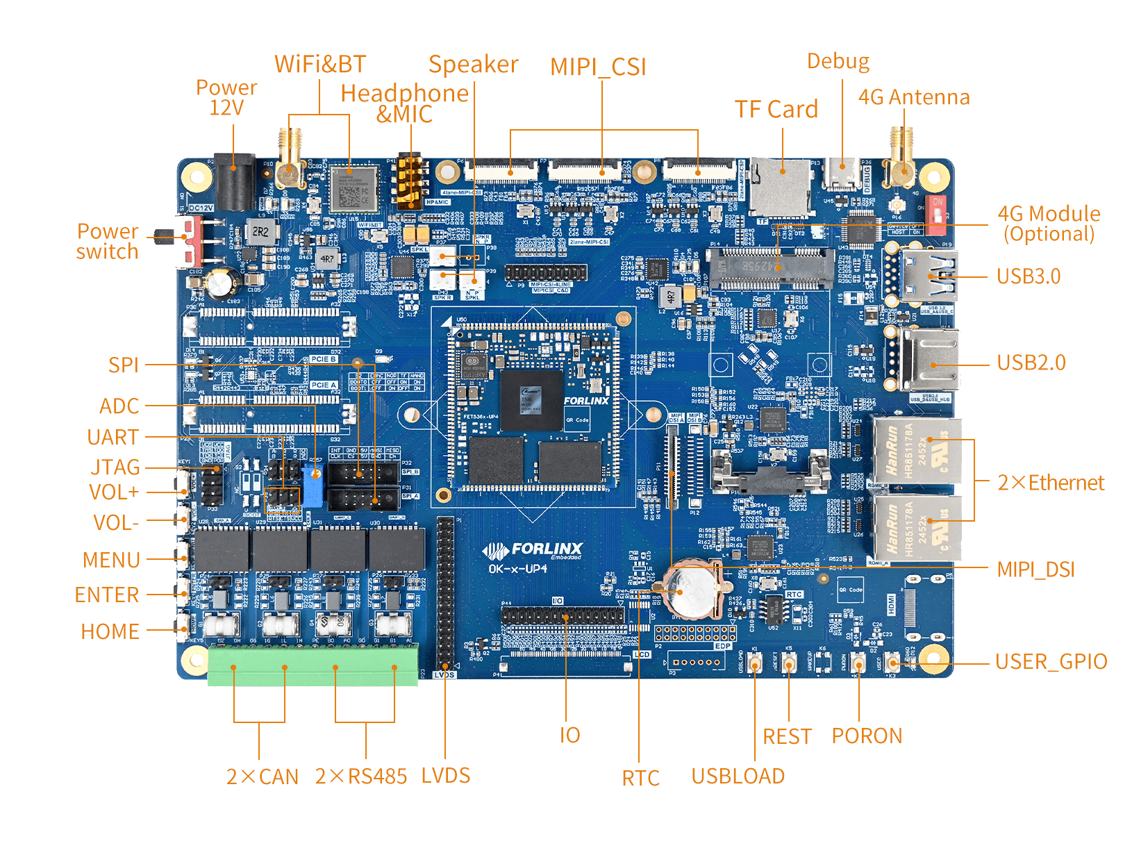
|
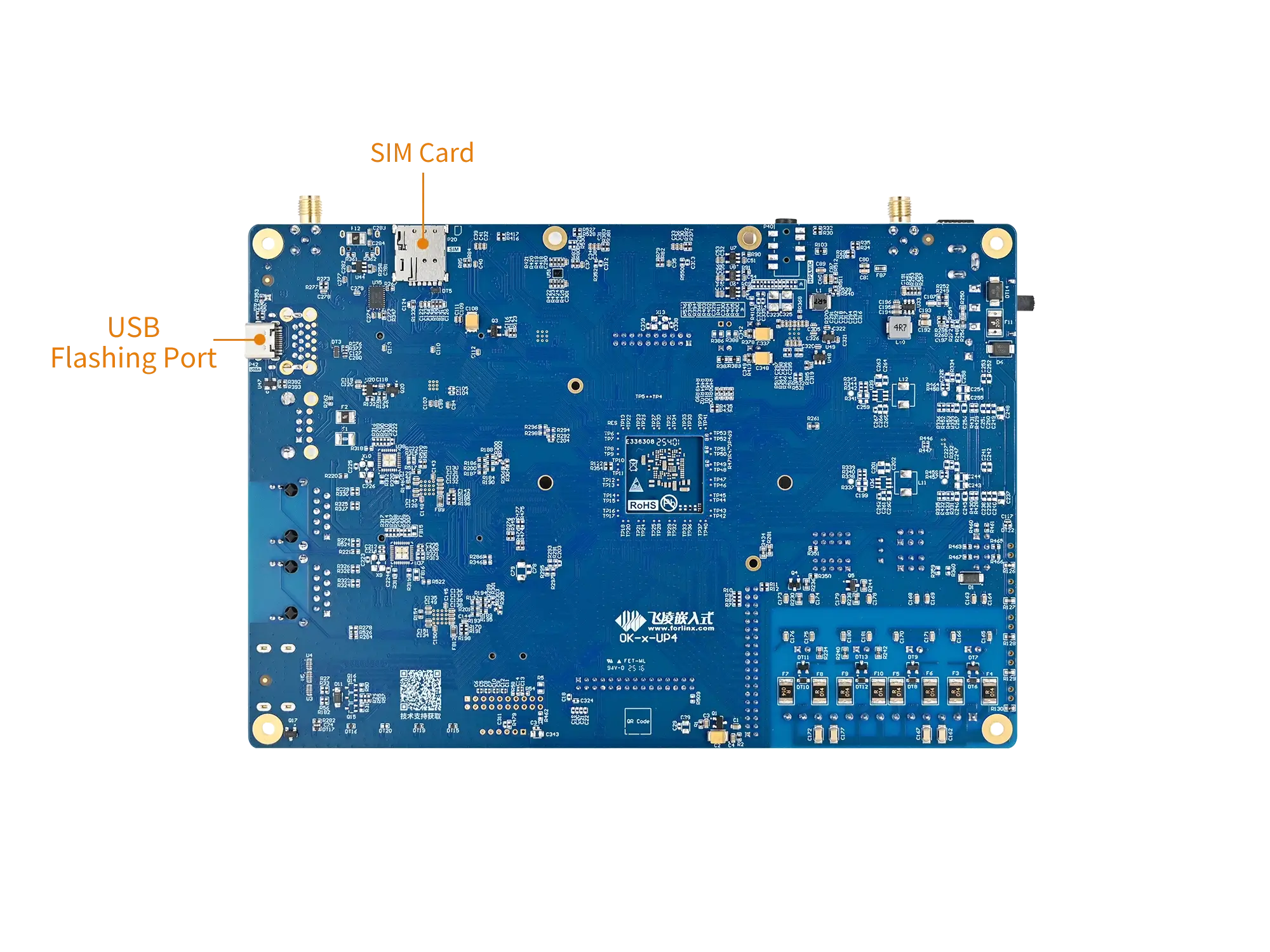
|
| OK536-UP4 Development Board Function Parameters | ||
|---|---|---|
| Function | Quantity | Parameter |
| WiFi & Bluetooth | 1 | Single antenna 2.4G & 5GHz Wi-Fi Dual-band 1X1 802.11ac + Bluetooth 4.2 |
| Audio | 1 | Mono speaker connector, class-D, 1.3 W; Stereo headphone output, 32 Ohm load; Headphone recording + on-board MIC recording |
| MIPI-CSI | 3 | FPC socket is led out, 4lane + 2lane + 2lane, of which 4lane can be connected to 4-to-4 analog camera module |
| TF Card | 1 | Support maximum SDR104 rate |
| 4G | 1 | 4G module supporting miniPCIE interface, with USB2.0 communication signal |
| UART Debug | 1 | Integrated in a Type-C port that can be connected to a computer for debugging |
| USB3.0 | 1 | USB_A can switch the master-slave mode and perform USB programming, while USB_C only supports the master mode. |
| USB2.0 | 1 | 1 x USB-D native USB2.0 and 1 x USB-HUB are led out |
| Ethernet | 2 | 2 x Gigabit ports led out via a standard RJ45 socket |
| MIPI-DSI | 1 | 4-lane MIPI-DSI, supports capacitive touch screen and backlight brightness adjustment. The maximum resolution of a single channel is 1920x1200@60fps. |
| RTC | 1 | On-board CR1220 battery, keep going when power is off |
| LVDS | 1 | 4-lane LVDS, supporting capacitive touch screen and backlight brightness adjustment, up to 1366 x 768@60fps |
| RS485 | 2 | Electrical isolation |
| CAN | 2 | Supports CAN2.0B, electrical isolation |
| ADC | 3 | The pin header pin-out functions, which can be connected to a sliding rheostat to collect voltage values. |
| SPI | 2 | Two SPI interfaces, which are led out from the simple bull seat and can be connected to the peripheral debugging function. |
| UART | 1 | 5 x UART, led out through pin headers. |
| JTAG | 1 | JTAG, led out through pin |
| KEY ADC | 5 | 5 keys are led out via 1 x LRADC |
▊ Accessories
Please click here to get more information about the supported modules and accessories.
▊ Documentation
Reference Manuals
Hardware Related
Product Datasheet
User Guide
Carrier Board Schematic
Carrier Board PCB
SoM Pinmux
Software & BSP
OS Image
Testing Demo
Source Code
Manual
Request a Quote
Fill out the form below for volume pricing or technical specifications. We'll get back to you within 24 hours.
▊ Ordering Information
1. Online Channels: We have an online store on Alibaba and DigiKey. Please contact us for details.
2. Direct Inquiry: For bulk orders, please email our sales team at [email protected].
3. Payment Method: Standard terms: 100% T/T (Telegraphic Transfer) in advance.
1. Dispatch Method: Orders are shipped via international express upon receipt of payment.
2. Lead Time: 5 working days for samples; 6 weeks for bulk orders.
3. Shipping Policy: Shipping and handling fees are the responsibility of the purchaser.
▊ Forlinx Recommended Products
Architecture: Octa-core ARM Cortex-A55 (4+4 cluster)
Frequency: CPU 1.8GHz/1.4GHz | RISC-V 200MHz | DSP 600MHz
RAM: 2GB/4GB LPDDR4
ROM: 16GB / 32GB eMMC
Architecture: Cortex-A55
Frequency: 1.8GHz,2.0GHz
RAM: 1GB / 2GB / 4GB / 8GB LPDDR4X
ROM: 8GB / 16GB / 32GB / 64GB eMMC
Architecture: 4×Cortex-A53
Frequency: [email protected]
RAM: 1GB/2GB LPDDR4
ROM: 8GB/16GB eMMC
Architecture: 2*A55+M33
Frequency: 1.7GHz
RAM: 1GB LPDDR4
ROM: 8GB eMMC