


Qualcomm QCS8275 System on Module - Forlinx FET8275AA-C 8-Core Industrial AIoT Platform with 40 TOPS NPU
Empower your next-generation industrial and edge AI applications with the Forlinx FET8275AA-C System on Module (SoM) / Computer on Module. Powered by the Qualcomm Dragonwing QCS8275AA processor with an 8-core heterogeneous architecture (2x Kryo Gold Prime + 2x Kryo Gold + 4x Kryo Silver) and an integrated 40 TOPS NPU, it delivers robust computing power for complex edge AI workloads.
Engineered for industrial connectivity, the FET8275AA-C integrates TSN Ethernet, PCIe Gen4, USB 3.1 Gen2 and a dedicated 4-core real-time subsystem for deterministic control. Qualified for -40°C to +85°C operation, it guarantees reliable performance to secure your long-term industrial deployment.
Highlights:
- 8-Core Kryo CPU: 2x Kryo Gold Prime @2.35GHz + 2x Kryo Gold @2.1GHz + 4x Kryo Silver @1.95GHz, with 12GB LPDDR5.
- 40 TOPS NPU: 40 INT8 TOPS (Dense) for edge AI, vision and robotics.
- 4-Core Real-Time Subsystem: Dedicated RTSS with 4x CAN-FD for deterministic control.
- TSN Ethernet & PCIe Gen4: 2.5GbE SGMII, PCIe Gen4 (2-lane + 4-lane), USB 3.1 Gen2.
- Rich Multimedia: 3x MIPI CSI, 1x MIPI DSI, 1x DP 1.4.
- Industrial Grade: -40°C to +85°C, 90mm x 73mm SoM, 699-pin Mirror Mezz connector.
Qualcomm Dragonwing QCS8275AA Industrial AIoT SoC
QCS8275AA is an octa-core industrial-grade SoC from the Qualcomm Dragonwing IQ-8 family. It combines an 8-core Kryo CPU, Adreno 623 GPU and VPU, a 40 TOPS NPU and a 4-core real-time subsystem, delivering a balanced mix of peak performance, power efficiency and deterministic real-time response for edge AI and industrial automation.
8-Core Heterogeneous Compute
The QCS8275AA pairs 2x Kryo Gold Prime @2.35GHz and 2x Kryo Gold @2.1GHz performance cores with 4x Kryo Silver @1.95GHz efficiency cores, complemented by 12GB LPDDR5 and 256GB UFS 3.1 storage—ideal for compute-intensive AIoT applications.
40 TOPS NPU Empowering AI Capabilities
The integrated NPU provides 40 Dense INT8 TOPS of dedicated AI compute, enabling on-device deep learning for defect detection, visual inspection, autonomous navigation and other latency-sensitive edge AI scenarios.
4-Core Real-Time Subsystem
Deterministic Control
Beyond the 8 application cores, a dedicated 4-core real-time subsystem (RTSS) with up to 68 GPIOs and 4x CAN-FD executes deterministic, low-latency control tasks alongside the main OS—perfect for industrial automation, motor control and time-sensitive networking.
TSN Ethernet & High-Speed I/O
1x RGMII and 1x SGMII (up to 2.5GbE) with TSN support for converged real-time traffic; PCIe Gen4 with 2-lane and 4-lane interfaces (RC + EP mode); USB 3.1 Gen2 and USB 2.0 for high-throughput industrial connectivity and expansion.
Rich Multimedia & Vision Interfaces
3x MIPI CSI configurable as D-PHY or C-PHY with up to 93 Gbps aggregate bandwidth, 1x MIPI DSI (up to 17 Gbps with C-PHY) and 1x DP 1.4 (32.4 Gbps) support multi-camera vision systems and high-resolution display pipelines.
▊ Hardware Features
| FET8275AA-C System On Module Basic Parameters | |
|---|---|
| Processor | Qualcomm QCS8275AA |
| ARM:2x Kryo Gold Prime @2.35GHz + 2x Kryo Gold @2.1GHz + 4x Kryo Silver @1.95GHz | |
| NPU:40 INT8 TOPS (Dense) | |
| GPU:Adreno 623 GPU | |
| VPU:Adreno 623 VPU | |
| RAM | 12GB LPDDR5 |
| ROM | 256GB UFS 3.1 |
| Operating Temperature | -40°C ~ +85°C |
| Operating Voltage | DC 24V |
| Connection | Mirror Mezz 699-pin board-to-board connector |
| OS | Linux 6.18.44 |
| Flashing | USB Type-C |
| TF card | |
| FET8275AA-C System On Module Function Parameters | ||
|---|---|---|
| Function | QTY | Spec. |
| MIPI DSI | 1 | 1 x MIPI DSI with VESA DSC v1.2 support; |
| D-PHY v1.2: 2.5 Gbps/lane on four lanes per port, 10 Gbps total; | ||
| C-PHY v1.1: 5.7 Gbps/trio on three trios per port, 17 Gbps total. | ||
| DP 1.4 | 1 | 1 x DisplayPort v1.4, 8.1 Gbps per lane, 32.4 Gbps aggregate port bandwidth. |
| MIPI CSI | 3 | 3 x MIPI CSI configurable as D-PHY or C-PHY mode; |
| D-PHY v1.2: 2.5 Gbps/lane, 4 lanes per port, 10 Gbps per port, up to 30 Gbps total; each 4-lane port can be split into 1-lane + 2-lane or 1-lane + 1-lane combinations; | ||
| C-PHY v1.2: 10.2 Gbps/trio, 3 trios per port, 31 Gbps per port, up to 93 Gbps total; each 3-trio port can be split into 1-trio + 2-trio, or three independent 1-trio ports. | ||
| I2S | Up to 8 | LS-I2S: 5 dedicated low-speed I2S, 2 multiplexed with high-speed I2S, plus 1 dedicated high-speed I2S reconfigurable as low-speed (up to 8 LS-I2S in total, max clock 24.576 MHz); |
| HS-I2S: up to 3, of which 2 are multiplexed with LS-I2S and can be configured as LS-I2S when needed (max clock 73.728 MHz). | ||
| PCIe | 2 | 1 x 2-lane PCIe Gen4: PCIe0 (RC + EP); |
| 1 x 4-lane PCIe Gen4: PCIe1 (RC + EP). | ||
| USB | 2 | 1 x USB 3.1 Gen2 – USB0 (HS + SS, supports device and host modes); |
| 1 x USB 2.0 – USB2 (HS, supports device and host modes). | ||
| eMMC | 1 | 1 x 8-bit eMMC 5.1 interface, max clock frequency 192 MHz. |
| RGMII | 1 | 1 x RGMII interface (RTSS domain). |
| SGMII | 1 | 1 x SGMII interface, up to 2.5GbE. |
| CAN-FD | Up to 4 | 4 x CAN-FD (RTSS domain). |
| QUP | 21 | MD domain: 16 QUP serial engines — UART (64B FIFO), all QUP SEs configurable as UART; |
| MD domain: HS UART (128B FIFO), QUP0_SE_2/3, QUP1_SE_2/3 configurable as HS UART; | ||
| MD domain: I2C master, all QUP SEs configurable as I2C; | ||
| MD domain: I3C, QUP0_SE_0/1, QUP1_SE_0/1 configurable as I3C; | ||
| MD domain: SPI master, all QUP SEs except QUP0_SE_7 and QUP1_SE_3 configurable as SPI master; | ||
| MD domain: SPI slave, QUP0_SE_4/5, QUP1_SE_4/5 configurable as SPI slave; | ||
| RTSS domain: 5 QUP serial engines — UART (64B FIFO), all QUP SEs configurable as UART; | ||
| RTSS domain: HS UART (128B FIFO), QUP0_SE_2/3 configurable as HS UART; | ||
| RTSS domain: I2C master, all QUP SEs configurable as I2C; | ||
| RTSS domain: SPI master, all QUP SEs configurable as SPI master; | ||
| RTSS domain: SPI slave, QUP0_SE_0/1 configurable as SPI slave. | ||
| QSPI | 1 | 1 x QSPI (up to 100 MHz). |
| GPIO (MD domain) | Up to 133 | Main domain supports 133 GPIOs (GPIO_0 to GPIO_132). |
| GPIO (RTSS domain) | Up to 68 | RTSS domain supports 68 GPIOs (RTSS_IO_0 to RTSS_IO_67). |
Note*: The parameters listed above are based on hardware design or theoretical CPU limits. Interfaces may be multiplexed; numbers represent maximum theoretical availability.
▊ Development Board Function Parameters
| Development Board Function Parameters | ||
|---|---|---|
| Function | QTY | Spec. |
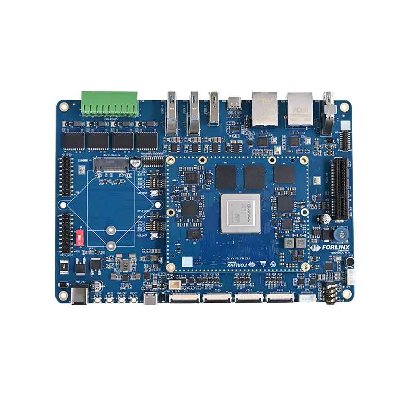
| MIPI DSI | 1 | Routed via FPC connector, default matching Forlinx 7-inch MIPI display at 1024x600@30fps. |
| DP 1.4 | 1 | Routed via DP port, default compatible with standard DP monitors. |
| MIPI CSI | 3 | Routed via 3 FPC connectors, default matching IMX577 camera modules. |
| Audio | 2 | 1 x I2S with MAX98357AETE+ amplifier, supporting 4Ω 1.3W / 8Ω 0.8W speakers; |
| 1 x I2S with codec chip, supporting speaker, headphone output and MIC input (TBD). | ||
| Type-C OTG | 1 | Type-C and Type-A switched via analog switch (S5 controls direction: OFF for Type-C, ON for Type-A); |
| System flashing uses the Type-C port. | ||
| USB 3.0 | 2 | Type-C and Type-A switched via analog switch (S5 controls direction: OFF for Type-C, ON for Type-A); |
| Type-A and 4G/5G module are onboard HUB expansion interfaces. | ||
| USB 2.0 | 1 | 1 x USB 2.0 Type-A port. |
| 4G/5G | 1 | Supports M.2 4G/5G module. |
| M.2 | 1 | 1 x M.2 KEY-E interface, 2-lane, default matching Wi-Fi & BT module. |
| PCIe | 1 | 1 x PCIe x1 slot (4-lane interface). |
| TF Card | 1 | Shares the SD interface, selected via 0Ω resistor. |
| eMMC | 1 | Shares the SD interface, selected via 0Ω resistor. |
| Ethernet | 2 | 1 x Ethernet port up to 1 GbE; 1 x Ethernet port up to 2.5GbE. |
| RS485 | 2 | 2 x RS485 ports with isolation and protection. |
| CAN-FD | 4 | 4 x CAN-FD ports with isolation and protection. |
| RTC | 1 | I2C interface, onboard RTC chip with button battery holder. |
| JTAG | 1 | JTAG debugging via pin header. |
| FAN | 1 | Fan connector for SoM cooling. |
| GPIO | n | Remaining MD_GPIO and RTSS_GPIO routed via FPC and pin headers for expansion. |
Note*: The parameters listed above are based on hardware design or theoretical CPU limits. Interfaces may be multiplexed; numbers represent maximum theoretical availability.
▊ Accessories
Please click here to get more information about the supported modules and accessories.
▊ Documentation
Reference Manuals
Product Brief
Hardware Documents
Product Datasheet
User Guide
SoM Pinmux
Carrier Board Schematic
Carrier Board PCB
Software Documents
Linux BSP User Guide
Driver Source Code
Driver Porting Guide
Flashing Guide (USB Type-C)
Request a Quote
Fill out the form below for volume pricing or technical specifications. We'll get back to you within 24 hours.
▊ Ordering Information
1. Online Channels: We have an online store on Alibaba and DigiKey. Please contact us for details.
2. Direct Inquiry: For bulk orders, please email our sales team at [email protected].
3. Payment Method: Standard terms: 100% T/T (Telegraphic Transfer) in advance.
1. Dispatch Method: Orders are shipped via international express upon receipt of payment.
2. Lead Time: 5 working days for samples; 6 weeks for bulk orders.
3. Shipping Policy: Shipping and handling fees are the responsibility of the purchaser.
▊ Forlinx Recommended Products
Architecture: 2x Kryo Gold Prime + 2x Kryo Gold + 4x Kryo Silver
Frequency: 2.35GHz + 2.1GHz + 1.95GHz
RAM: 12GB LPDDR5
ROM: 256GB UFS 3.1